The technological progress of the past decade has been amazing. If there is no important part as the cornerstone: PCB and PCBA, these feats of human genius and innovation will be meaningless.
We will study together what makes them different and how to distinguish them.
1. PCB vs PCBA-what is PCB? The meaning of /PCB PCB (printed circuit board) is a key module used to connect electronic components. The board utilizes pads, conductive traces, and other copper etch features to effectively promote the functionality of electrical devices.
Then, the electronic component specialist is individually placed on the substrate and soldered to the appropriate interconnection circuit. The substrate has "contact fingers" along the edges, which are used to connect to external devices or even other PCBs.
Most of the electrical equipment we use now uses PCBs. From basic equipment such as radios and pagers to complex instruments such as radar equipment and computers. Depending on the needs, the PCB circuit can be configured to perform single or multiple functions.
1.1 Types of PCB
Now that you know what a PCB is, you should know that we have more than one type of PCB. PCB is mainly divided into three types, namely:
·Single-sided PCB
All components of a single-sided PCB are mounted on only one side of the circuit board. The correct structure can ensure that all components are installed in the proper position and fixed.

·Double-sided PCB
When there are too many components to be placed for a single side, use a double-sided PCB. The electrical connection between the two sides is achieved by drilling directly through the base plate at key locations. The internal pores are coated with conductive material to achieve high-efficiency current.
·Multilayer PCB
The continuous printed circuit layers are mutually designed with multilayer boards; separated by insulating material layers. Connect the components on the surface to the appropriate circuit by drilling plated holes in the desired layer.
PCBs are vital to all aspects of our daily lives. The appliances and resources we use to keep our lives running are based on printed circuit boards. Read on to learn how this amazing technical design is designed.
1.2 Design
The PCB design offers unlimited possibilities. Each board is designed to perform a specific function for a unique product. For PCB design, experts use CAD (Computer Aided Design) systems and special software to lay out the circuit patterns of the circuit board. The circuit board designer must be able to allocate space for the circuit board to the maximum extent and realize the required functions.
After the circuit is laid out, the negative image of the design (mask) is printed on a transparent plastic board with precise dimensions. The mask paints black areas that are not part of the design; the circuit appears clear in the background. The location of the contact hole is also easy to distinguish from the overall design.
1.3 PCB vs PCBA-commonly used materials
You already understand the key processes involved in PCB design. It is surprising how a small number of technologies have such a powerful impact. The importance of PCB means that only the best and most durable materials are used to make it. Read on to understand the components of a PCB.
In PCB manufacturing and printing, the substrate material used is usually glass fiber reinforced epoxy resin. High-end board production involves pairing glass fiber-reinforced epoxy with copper foil bonded to one or both sides of the substrate.
Use paper-reinforced boards made of phenolic resin and affixed with copper foil; often cheaper. These PCBs are easily found in household appliances.
The printed circuit of the circuit board is made of copper. The material is etched or plated on the surface of the substrate in a desired pattern. To prevent oxidation of copper circuits, they are coated with tin-lead to provide the required protection.
The contact fingers on the outer edge of the substrate are first plated with a tin-lead mixture, then nickel, and finally gold for maximum conductivity.
I believe we have covered all knowledge about PCB. However, this is only one side of the coin. In the next chapter, we will delve into what is printed circuit board assembly) which is the circuit board that appears after the entire parts and components are soldered and installed correctly. PCBA and why it is so important.
2. PCB vs PCBA-what is PCBA?
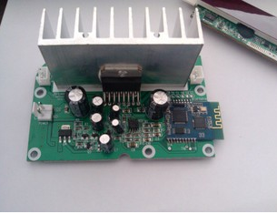
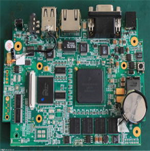
Printed circuit board assembly) is the circuit board that appears after the entire parts and components are soldered and properly installed. PCBA stands for printed circuit board assembly. It refers to the board obtained after all printing and installation operations are completed. When choosing PCB and PCBA, the key point to note is that PCB is just a printed circuit board. PCB rapid prototyping. 3D PCB printing can not only make PCBs, but also make printed circuit board assembly. PCBA is a complete package; it is already equipped with all the necessary components and is ready to be deployed for its intended purpose.
2.1 Circuit board
There are two main methods for assembling components in PCB rapid prototyping. 3D PCB printing not only manufactures PCBs, but also performs printed circuit board assembly (PCBA. They are:
·Surface Mount Technology (SMT)
This PCB rapid prototyping method. 3D PCB printing not only makes PCBs, but also assembles printed circuit boards (PCBA is very suitable for small-sized circuits and components. It is a fully automatic SMT). This will allow the placement machine to easily place the components on the PCB (the PCB assembly process has three main steps. First, the printed circuit board gets a large amount of high-quality solder paste from the printer. Next), install all the necessary components In their respective locations. Finally, the circuit board passes through a 500-degree furnace to liquefy the solder paste, thus sealing all components in place.
·PCB vs PCBA--Through Hole Device (THD)
THD technology combines manual and automatic operations. It also involves three execution steps. The first step requires the technician to manually place the components on the circuit board. The second step deals with the inspection and rectification of all set components. In the third step, the entire PCB assembly is wave soldered. Wave soldering is the process of passing the assembled circuit board through a wave of liquid solder at 500 degrees Fahrenheit.
3. PCB vs PCBA
So far, we have understood what PCB is and the principle of PCB rapid prototyping. 3D PCB printing not only manufactures PCBs, but also performs printed circuit board assembly (PCBA work. With this important knowledge, it is time to find the differences and what makes them unique.
PCB rapid prototyping. 3D PCB printing not only manufactures PCBs, but also performs printed circuit board assembly (PCBA can be regarded as a complete board and can only be manufactured after the PCB is fully developed.
3.1 PCB and PCBA-Difference
It is important to be able to spot the differences between PCB and PCB rapid prototyping. 3D PCB printing not only makes PCB, but also makes printed circuit board assembly (PCBA. The main differences are:
·Production Process
PCB (Printed Circuit Board) is easier to produce; because it does not require assembly. And PCB rapid prototyping. 3D PCB printing makes the PCB, but it also makes the printed circuit board assembly (PCBA) more complicated due to the various components that need to be connected and the subsequent furnace soldering their connections.
·cost
For the same board, the cost of manufacturing a PCB is much lower than the cost of producing a rapid prototype of a PCB. 3D PCB printing not only manufactures PCBs, but also manufactures printed circuit board assemblies (PCBAs. Additional components attached to the PCBA will incur a lot of costs, thereby increasing the overall cost of the complete PCBA.
·Function
The PCB is a "blank board". It has no components that facilitate the passage of electric current. On the other hand, PCBA has all the basic components and is ready for deployment.
·Package
PCB adopts vacuum packaging, while PCBA board adopts compartment or anti-static packaging.
3.2 PCB vs PCBA-Application
The application of PCB extends to all electrical equipment we use. From simple pagers and alarms to complex types of machinery such as MRI and radar equipment. As we know, modern society operates on the basis of the film production work you need to make PCBs. In the case of PCBA. Our cars, media equipment and home appliances will all be imaginary luxury items; if we do not have printed circuit boards (PCB) and printed circuit board assemblies (PCBA).
in conclusion
There is no doubt that the PCB is an essential part of all electrical systems. Our society relies on the continuous performance of circuit boards to run our affairs efficiently. If this basic technology fails, all human systems that run on electricity will be unusable.
Overall, there are some exciting prospects for the development of PCB and PCBA in the future. We are steadily moving towards more optimized designs and the ability to pack super-complex functions into miniature circuit boards.