Nowadays, the electronic processing industry in mainland China is very prosperous. As a professional processing company, it is natural that the faster the order is completed, the better. The following will explain how to effectively reduce the PCB proofing time.
First, for the electronic processing industry, there are often urgent orders, and if you want to effectively reduce the time of PCBA proofing, first of all, don't spend time on things other than proofing homework, just like before the proofing. Carefully read the documentation of PCBA proofing, determine the requirements for the entire proofing, and then prepare the materials needed in advance, and arrange the proofing staff. If two shifts are required, staff attendance and shifts should be arranged. Make sure that all preparatory tasks except technology are completed.

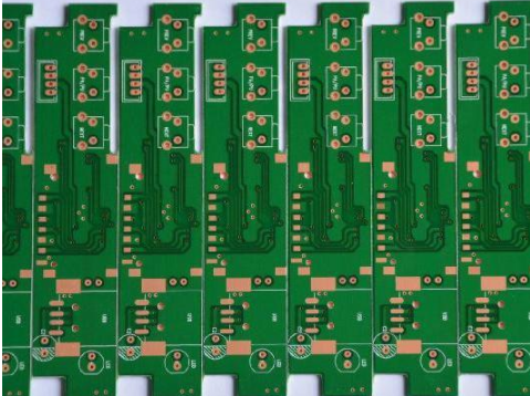
Secondly, the planning of PCB proofing schemes should be more standardized. Usually the professional PCB proofing time is five days to half a month. The reason for the large difference in time is most likely because the design scheme is not standardized in the calculation of the design time. This caused the manufacturer to take a detour during production, so the design plan should be standardized, such as how many cooling holes should be reserved for the circuit board, and where the marking position of the silk screen is. It may be just the parameters written in the design plan, but Can effectively reduce PCBA proofing time.
Third, it is also very important to control the number of PCBA proofings. If the number planned at the beginning is too large, it will lead to cost improvement, but try to make more PCBA proofings as possible due to the performance test. At that time, there was a burning board situation.
The above points are ways to reduce the time of PCBA proofing. In addition, the efficiency of PCBA proofing is also related to factors such as technical experience, so as a processing company, it should be promoted technically.
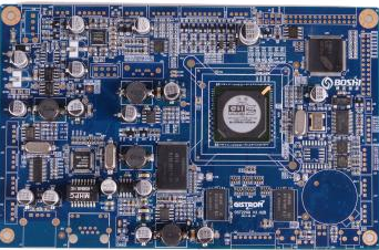
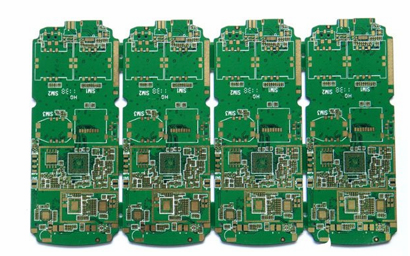
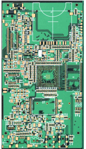
What method is used for PCBA proofing?
1. Subtraction method. This kind of method mainly uses chemicals to remove the unnecessary places on the vacant circuit boards, and the remaining places are the necessary circuits. PCBA design and processing mainly use screen printing or photosensitive plates and engraving for processing. Remove unnecessary departments.
2. Additive method. This kind of method is to expose the necessary places through the combination of ultraviolet light and photoresist, and then use electroplating to thicken the certificate circuit, and then cover with anti-etching resist or metal thin tin, and finally cover the photoresist and the cage The copper foil layer is etched away.
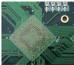
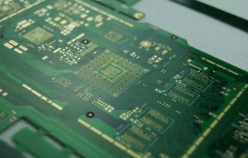
3. Multilayer method. This type of method is the most common method for PCB design and processing, and it is also the main method for making multilayer printed circuit boards. It is through the process from the inner layer to the outer layer, and then using the subtractive or additive method to process, the process of repeating the layering method continuously, so as to realize the production of multi-layer printed circuit boards. The most pivotal process is the build-up method, where the printed circuit boards are added layer by layer and repeated processing is performed.