In sports, there is a well-known connection between strength and speed. Basically, power or strength is the determinant of movement speed. However, at a certain point, there is no longer this positive correlation between strength (closely related to muscle size) and speed, and increasing size and strength will actually slow down your speed. Similarly, in the not-too-distant past, productivity and efficiency had a comparable relationship in manufacturing.
Today, the most advanced manufacturing facilities are highly automated. The reduction in reliance on human repetitive ability improves efficiency and productivity, and makes these two indicators more closely aligned with process speed. This is indeed the right best printed circuit board assembly (PCBA) equipment capabilities and process technology to determine productivity and efficiency. Ensuring that the circuit board design is reasonable and following the design of good assembly (DFA) guidelines can minimize the need for manual intervention. Let's review the process to help determine the design focus areas to maximize PCBA speed.

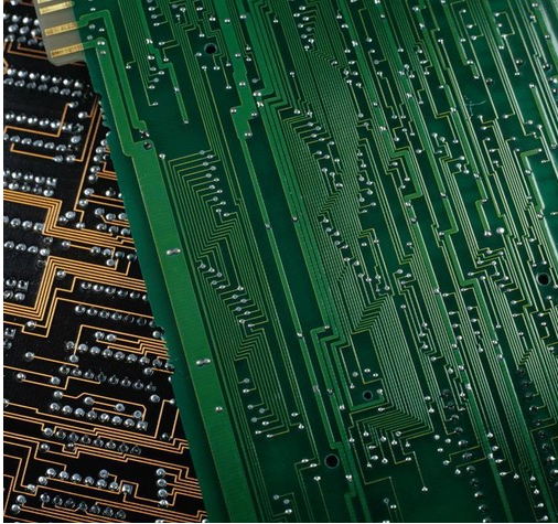
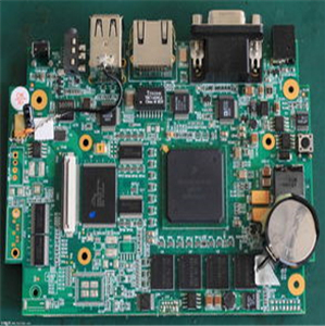
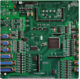
Printed circuit board assembly (PCBA) process
Transforming your design into a complete physical structure requires three steps: 1) manufacturing, 2) component procurement and 3) assembly. Printed circuit board assembly or PCBA is one of two PCB manufacturing processes. The other stage is manufacturing, which is executed first. During the manufacturing process, your circuit board design is complete and ready for assembly, where the components are firmly connected to the board. Although PCBA may contain ten or more steps, the process can be divided into the following main tasks:
Prepare
Before placing surface mount technology (SMT) components, an initial layer of solder paste is applied to the pads on the circuit board. This is done to promote good flow during the welding process and minimize assembly defects. The coating method can be manual or an automated method using stencil printing or jet printing.
Component placement
For SMT components, accurate placement of the components on the pads is critical. Improper alignment may cause poor solder joints or tombstones to fall off, where one side of the component is not connected to the board. Through-hole technology (THT) components are more flexible; however, it is generally recommended that the component body be as close to the board surface as possible.
welding
The most common method for fixing SMT components is reflow soldering. For THT components, wave soldering is the preferred method. If two types of components are used at the same time, the SMT components are usually placed and soldered first. Only in this way, THT components are placed and welded, which expands the welding task. Since the components are installed on the top and bottom surfaces, the welding of double-sided circuit boards is further expanded. After the soldering steps for each component type are completed, the connection will be checked, and if any problems are found, rework is required for correction.
clean
Clean to remove all excess debris from the surface of the circuit board. Alcohol or deionized water can effectively remove most contaminants.
Depanelization
Splitting is the work of dividing a multi-board panel into individual units or PCBs. It is the final main task and should not be ignored. Panelization or inefficient panel design will result in a lot of waste and additional costs.
The above tasks are determined by your contract manufacturer (CM) and the quality of the manufacturing process depends on your choice of manufacturing and assembly services. However, certain design strategies can be used to optimize PCBA, especially in terms of speed.
Design circuit boards to optimize PCBA speed
Any design decision made with the goal of improving PCBA can and should be part of the DFA guidelines. These include options aimed at improving the efficiency, quality or speed of the process. Especially in order to increase the speed, we can define a list of specific tasks, and if the list is executed during the design process, the process can be optimized.
PCB assembly speed optimization checklist
Planning stage
Prioritization Speed When selecting CM and assembly services.
Procurement stage
Select components can be used throughout the development process.
Eliminate or minimize the use of through-hole components.
Layout a Panelized design minimizes waste and scores where possible to achieve quick and easy separation.
Manufacturing stage
Use CM's default materials, solder resist and screen printing colors, and surface finish.
Ensure that your design package is complete and accurate, including BOM, engineering drawings and any special information, and is the best format for CM.