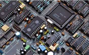
PCBA processing components have different requirements
The layout of the components in PCBA processing affects the quality of the SMT process, so when the components are laid out, they need to be done in accordance with the relevant process requirements. The correct layout design can minimize soldering defects and ensure product quality. The following PCBA processing factory editor will organize and introduce the layout requirements of PCBA processing components for everyone.
1. Layout requirements of components:
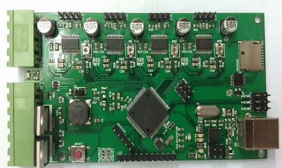
1. The components on the PCB are arranged as regularly and evenly as possible. For components of the same type of package, the orientation, polarity, and spacing should be consistent as much as possible. The regular arrangement is convenient for inspection and helps to increase the patch/plug-in speed; even distribution is good for the optimization of heat dissipation and welding process.
2. The power components should be evenly placed on the edge of the PCB or on the ventilated position in the chassis to ensure good heat dissipation.
3. Do not place valuable components on the corners, edges of the PCB, or close to connectors, mounting holes, slots, cutting, gaps and corners of the puzzle, these locations are high stress areas of the PCB, which are likely to cause solder joints. And cracking of components.
4. Leave a certain maintenance gap around the large components in PCBA processing(leave the size of the heating head of the SMD rework equipment that can be operated).
5. The layout of components on the wave soldering surface should meet the following requirements:

1) Suitable for wave soldering, such as Chip type SMD components (SMD resistors, SMD capacitors, SMD inductors), SOT, SOP (lead center distance P≥1.27mm) with a package size greater than or equal to 0603 (metric 1608) and above ), etc., fine-pitch devices cannot be placed.
2) The height of the component should be less than the wave height of the wave soldering equipment.
3) The extension direction of the component leads should be perpendicular to the PCB transfer direction during wave soldering, and two adjacent components must meet a certain distance requirement.
4) The package of components on the soldering surface of wave soldering must be able to withstand temperatures above 260°C and be fully sealed.
2. Component assembly method requirements:
The so-called assembly method refers to the layout of components on the front and back sides of the PCB. The assembly method determines the assembly process flow. According to the characteristics of the SMT process flow, the general assembly methods mainly include the following four:
1) When single-sided mixed mounting is used, the placement and insertion components should be placed on the first side.
2) When using double-sided mixed mounting, the large mounting and inserting components should be placed on the first side, and the large components on both sides of the PCB should be staggered as much as possible.
The layout of components in PCBA processing is very important, because product quality problems caused by unreasonable layout design are difficult to overcome in production, so it is necessary to control from the source and arrange the components reasonably according to requirements.