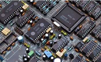
Analysis on the key points of PCBA failure technology
As the carrier of various components and the hub of circuit signal transmission,PCB has become the most important and critical part of electronic information products. Its quality and reliability determine the quality and reliability of the entire equipment. However, due to cost and technical reasons, a large number of failure problems have occurred in the production and application of PCB.
It takes so long to use some common failure analysis techniques. Between the structural characteristics of the PCB and the main failure modes, this article will focus on nine techniques for PCB failure analysis, including: visual inspection, X-ray fluoroscopy, metallographic section analysis, thermal analysis, photoelectron spectroscopy, display Micro-infrared analysis, scanning electron microscope analysis and X-ray energy spectrum analysis, etc. Metallographic section analysis is a destructive analysis technique. Once these two techniques are used, the sample is destroyed and cannot be recovered; in addition, due to the requirements of sample preparation, scanning electron microscopy and X-ray energy spectrum analysis may sometimes be required Partially destroy the sample. In addition, in the process of analysis, due to the need for verification of failure location and failure reasons, it may be necessary to use test techniques such as thermal stress, electrical performance, solderability testing and size measurement, etc., which will not be specifically introduced here. .
1. Visual inspection
Appearance inspection is to inspect the appearance of PCB visually or using some simple instruments, such as stereo microscope, metallographic microscope or even magnifying glass, to find the failure parts and related physical evidence. The main function is to locate the failure and initially determine the failure mode of the PCB. The visual inspection mainly checks the PCB pollution, corrosion, the location of the board burst, the circuit wiring and the regularity of the failure, if it is batch or individual, is it always concentrated in a certain area, etc. In addition, many PCB failures are discovered after being assembled into PCBA. Whether the failure is caused by the influence of the assembly process and the materials used in the process also requires careful inspection of the characteristics of the failure area.
2. X-ray fluoroscopy
For some parts that cannot be visually inspected, as well as the internal and other internal defects of the through holes of the PCB, X-ray fluoroscopy system has to be used for inspection. X-ray fluoroscopy systems use different material thicknesses or different material densities based on different principles of moisture absorption or transmittance of X-rays for imaging. This technology is more used to check the internal defects of PCBA solder joints, the internal defects of through-holes, and the positioning of defective solder joints of BGA or CSP devices in high-density packaging. The resolution of the current industrial X-ray fluoroscopy equipment can reach one micron or less, and it is changing from two-dimensional to three-dimensional imaging equipment. There are even five-dimensional (5D) equipment used for package inspection, but this 5D X The optical perspective system is very expensive and rarely has practical applications in the industry.
Three, slice analysis
Slicing analysis is the process of obtaining the cross-sectional structure of the PCB through a series of methods and steps such as sampling, inlaying, slicing, polishing, corrosion, and observation. Through slice analysis, we can get rich information of the microstructure that reflects the quality of PCB (through holes, plating, etc.), which provides a good basis for the next quality improvement. However, this method is destructive. Once sliced, the sample will inevitably be destroyed. At the same time, this method requires high sample preparation and takes a long time to prepare the sample, which requires well-trained technicians to complete. For detailed slicing process, please refer to the process specified in IPC-TM-650 2.1.1 and IPC-MS-810.
Four, scanning acoustic microscope
At present, the C-mode ultrasonic scanning acoustic microscope is mainly used for electronic packaging or assembly analysis. It uses the amplitude, phase and polarity changes generated by the reflection of high-frequency ultrasonic waves on the discontinuous interface of the material to image. The scanning method is along the The Z-axis scans the information on the X-Y plane. Therefore, the scanning acoustic microscope can be used to detect various defects in components, materials, and PCBs and PCBAs, including cracks, delamination, inclusions, and voids. If the frequency width of the scanning acoustics is sufficient, the internal defects of the solder joints can also be directly detected. A typical scanning acoustic image uses a red warning color to indicate the existence of defects. Because a large number of plastic packaged components are used in the SMT process, a large number of moisture reflow sensitivity issues are generated during the conversion from lead to lead-free process. That is to say, moisture-absorbing plastic packaged devices will experience internal or substrate delamination cracking during reflow at a higher lead-free process temperature, and common PCBs will often explode under the high temperature of the lead-free process. At this time, the scanning acoustic microscope highlights its special advantages in non-destructive testing of multilayer high-density PCBs. Generally, obvious bursts can be detected only by visual inspection of the appearance.

5. Micro-infrared analysis
Micro-infrared analysis is an analysis method that combines infrared spectroscopy and microscope. It uses the principle of different absorption of infrared spectra by different materials (mainly organic matter) to analyze the compound composition of the material, and combined with the microscope can make visible light and infrared light the same. The light path, as long as it is in the visible field of view, you can find the trace organic pollutants to be analyzed. Without the combination of a microscope, infrared spectroscopy can usually only analyze samples with a large amount of samples. However, in many cases in electronic technology, micro-pollution can lead to poor solderability of PCB pads or lead pins. It is conceivable that it is difficult to solve process problems without infrared spectroscopy with a microscope. The main purpose of micro-infrared analysis is to analyze the organic contaminants on the welded surface or the surface of the solder joint, and analyze the cause of corrosion or poor solderability.
6. Scanning electron microscope analysis
Scanning electron microscope (SEM) is one of the most useful large-scale electron microscopy imaging systems for failure analysis. Its working principle is to use the electron beam emitted from the cathode to be accelerated by the anode and to form a beam with a diameter of tens to With an electron beam current of several thousand angstroms (A), under the deflection of the scanning coil, the electron beam scans the surface of the sample point by point in a certain time and space sequence. This high-energy electron beam bombards the surface of the sample and will excite A variety of information is output, and various corresponding graphics can be obtained from the display screen after collection and magnification. Excited secondary electrons are generated in the range of 5~10nm on the sample surface. Therefore, secondary electrons can better reflect the morphology of the sample surface, so they are most commonly used for morphology observation; while the excited backscattered electrons are generated on the sample surface In the range of 100~1000nm, the backscattered electrons with different characteristics are emitted according to the atomic number of the substance. Therefore, the backscattered electron image has the morphological characteristics and the ability to distinguish the atomic number. Therefore, the backscattered electron image can reflect the chemical element. Distribution of ingredients. The current scanning electron microscope has very powerful functions. Any fine structure or surface feature can be magnified to hundreds of thousands of times for observation and analysis.
In the failure analysis of PCB or solder joints, SEM is mainly used to analyze the failure mechanism. Specifically, it is used to observe the topographic structure of the pad surface, the metallographic structure of the solder joint, measure the intermetallic compound, and the solderability coating Analyze and do tin whisker analysis and measurement. Unlike the optical microscope, the scanning electron microscope produces an electronic image, so only black and white. The sample of the scanning electron microscope needs to be conductive, and the non-conductor and some semiconductors need to be sprayed with gold or carbon. Otherwise, the accumulation of charges on the surface of the sample will affect Observation of the sample. In addition, the depth of field of the scanning electron microscope image is far greater than that of the optical microscope, and it is an important analysis method for uneven samples such as metallographic structure, microscopic fracture and tin whisker.
Seven, X-ray energy spectrum analysis
The scanning electron microscope mentioned above is generally equipped with an X-ray energy spectrometer. When a high-energy electron beam hits the surface of the sample, the inner electrons in the atoms of the surface material are bombarded and escaped. When the outer electrons transition to a lower energy level, characteristic X-rays will be excited, which is characteristic of different atomic energy levels of different elements. X-rays are different. Therefore, the characteristic X-rays emitted by the sample can be analyzed as the chemical composition. At the same time, according to the detection X-ray signal as the characteristic wavelength or characteristic energy, the corresponding instruments are called spectral dispersion spectrometer (abbreviated as spectrometer, WDS) and energy dispersion spectrometer (abbreviated as energy spectrometer, EDS), and the resolution of the spectrometer It is higher than the energy spectrometer, and the analysis speed of the energy spectrometer is faster than that of the spectrometer. Due to the fast speed and low cost of the energy spectrometer, the general scanning electron microscope configuration is the energy spectrometer.
With the different scanning methods of the electron beam, the energy spectrometer can perform surface point analysis, line analysis and surface analysis, and can obtain information about the different distribution of elements. Point analysis obtains all elements of a point; line analysis performs one element analysis on a specified line each time, and scans multiple times to obtain the line distribution of all elements; surface analysis analyzes all elements in a specified surface, and the measured element content is Average value of measuring area
In the analysis of PCB, energy spectrometer is mainly used for the component analysis of the surface of the pad, and the element analysis of the surface contaminants of the pad and the lead pin with poor solderability. The accuracy of the quantitative analysis of the energy spectrometer is limited, and the content of less than 0.1% is generally not easy to detect. The combined use of energy spectroscopy and SEM can obtain information on surface morphology and composition at the same time, which is why they are widely used.
8. Photoelectron Spectroscopy (XPS)
When the sample is irradiated by X-rays, the inner shell electrons of the surface atoms will break away from the bond of the atomic nucleus and escape the solid surface to form electrons. Measuring the kinetic energy Ex, the binding energy Eb of the inner shell electrons of the atoms can be obtained. Different electron shells vary. It is the "fingerprint" identification parameter of the atom, and the resulting spectrum is the photoelectron spectroscopy (XPS). XPS can be used for qualitative and quantitative analysis of elements on the shallow surface (several nanometers) of the sample surface. In addition, information about the chemical valence of elements can also be obtained based on the chemical shift of the binding energy. It can give information about the surface layer atomic valence state and the bonding of surrounding elements; the incident beam is an X-ray photon beam, so it can be analyzed for insulating samples without damaging the analyzed sample for rapid multi-element analysis; it can also be used in the case of argon ion stripping Longitudinal element distribution analysis is performed on multiple layers (see the following case), and the sensitivity is much higher than that of the energy spectrum (EDS). XPS is mainly used for the analysis of the quality of the coating of the pad, the analysis of the pollutants and the analysis of the oxidation degree in the analysis of the PCB to determine the deep-seated causes of poor solderability.
Nine, thermal analysis differential scanning calorimetry
(Differential Scanning Calorim- etry): A method of measuring the power difference between the input material and the reference material and the temperature (or time) relationship under program temperature control. DSC is equipped with two sets of compensation heating wires under the sample and reference container. When the temperature difference ΔT between the sample and the reference occurs due to the thermal effect during the heating process, the differential thermal amplifier circuit and the differential heat compensation amplifier can be used, Make the current flowing into the compensation heating wire change, balance the heat on both sides, the temperature difference ΔT disappears, and record the difference between the heating power of the two electric heating compensation under the sample and the reference object with the temperature (or time) change relationship, according to This change relationship can be used to study and analyze the physical, chemical and thermodynamic properties of materials. DSC has a wide range of applications, but in PCB analysis, it is mainly used to measure the degree of curing of various polymer materials used on the PCB (for example, Figure 2) and the glass transition temperature. These two parameters determine the PCB in the subsequent process. Reliability.
Thermomechanical Analyzer (TMA): Thermomechanical Analysis Technology (Thermal Mechanical Analysis) is used to measure the deformation performance of solids, liquids and gels under thermal or mechanical force under program temperature control. Common load methods include compression, needle Insertion, stretching, bending, etc. The test probe is supported by a cantilever beam and a coil spring fixed on it, and a load is applied to the sample through a motor. When the sample is deformed, the differential transformer detects this change and processes it together with data such as temperature, stress and strain. The relationship between the deformation of the material and the temperature (or time) under negligible load can be obtained. According to the relationship between deformation and temperature (or time), the physical, chemical and thermodynamic properties of materials can be studied and analyzed. TMA has a wide range of applications. It is mainly used for the two most critical parameters of PCB in PCB analysis: measuring its linear expansion coefficient and glass transition temperature. PCBs with substrates with too large expansion coefficients often lead to fracture failure of the metallized holes after soldering and assembly.
Due to the high-density development trend of PCB and the environmental protection requirements of lead-free and halogen-free, more and more PCBs have various failure problems such as poor wetting, cracking, delamination, CAF and so on. Introduce the application of these analysis techniques in actual cases. The acquisition of the failure mechanism and causes of the PCB will be beneficial to the quality control of the PCB in the future, so as to avoid the recurrence of similar problems.