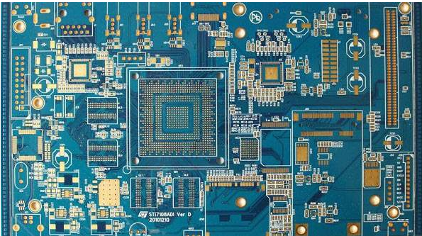
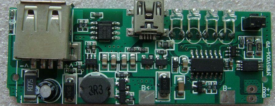
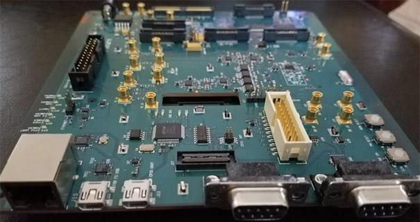
Explain PCB manufacturing and processing parameters
At present, the country has higher and higher requirements for environmental protection and greater efforts in link governance. This is a challenge but also an opportunity for PCB factories. If PCB factories are determined to solve the problem of environmental pollution, then FPC flexible circuit board products can be at the forefront of the market, and PCB factories can get opportunities for further development.
The Internet era has broken the traditional marketing model, and a large number of resources have been gathered together to the greatest extent through the Internet, which has also accelerated the development speed of FPC flexible circuit boards, and then as the development speed accelerates, environmental problems will continue to appear in PCB factories. In front of him. However, with the development of the Internet, environmental protection and environmental informatization have also been developed by leaps and bounds. Environmental information data centers and green electronic procurement are gradually being applied to the actual production and operation fields.
In the design, from the perspective of PCB board assembly, the editor believes that the following parameters should be considered:
1. The diameter of the hole should be determined according to the maximum material condition (MMC) and the minimum material condition (LMC). The diameter of a hole of an unsupported component should be selected such that the MMC of the pin is subtracted from the MMC of the hole, and the difference is between 0.15-0.5 mm. And for ribbon pins, the difference between the nominal diagonal of the pin and the inner diameter of the unsupported hole will not exceed 0.5mm and not less than 0.15mm.

2. Place smaller components reasonably so that they will not be covered by larger components.
3. The thickness of the solder mask should not be greater than 0.05mm.
4. The screen printed logo cannot intersect with any pads.
5. The upper half of the circuit board should be the same as the lower half to achieve structural symmetry. Because an asymmetrical circuit board may bend.
We design (if you need), manufacture, and ship electronic products that customers need, and provide customers with one-stop comprehensive solutions to help customers get rid of cumbersome production, solve their worries, and enable customers to focus more on market business development . We deeply understand that quality, price, and delivery time play a key role in improving the competitiveness of customers in the market. We have also spared no effort to help customers achieve this goal. Excellent quality, high-quality price, and on-time delivery are our service commitments. For this reason, we have won a good reputation in the field of electronic manufacturing services and won the trust of customers, which makes customers feel relieved to hand over projects one after another. We work together.
Paying attention to the trend of environmental protection informatization and the development of various environmental protection technologies, PCB factories can start with big data to monitor the company's pollution discharge and governance results, and find and solve environmental pollution problems in a timely manner. Keep up with the production concept of the new era, continuously improve resource utilization, and realize green production. Efforts to make the PCB factory industry realize an efficient, economical and environmentally friendly production model, and actively respond to the country's environmental protection policy.