A newly designed circuit board becomes PCBA after SMT, wave soldering or manual soldering, which is the first step in the long march. However, from PCBA to final finalization and delivery to the factory for mass production, a series of tests and verifications are required in the middle. Many young electronic engineers are not clear about PCBA and electronic product system debugging steps and specific requirements at each stage, which often leads to inefficient development and debugging, and even damages the circuit board to be tested. What is even more frightening is that the design with functional or performance defects is transferred to the mass production stage, causing huge losses to the company. Based on years of personal practice, the author summed up the nine steps from PCBA to product finalization, and efficiently completed the research and development of a variety of electronic products.
First step visual inspection
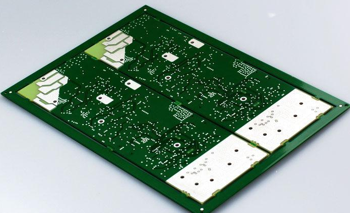
The PCBA that has just been mounted and delivered to the electronic engineer is shown in Figure 1. Experienced engineers can quickly find many design, material and process problems through visual inspection, which can save a lot of follow-up debugging time.

1.1. Carefully compare the circuit diagram, check whether the version of the schematic diagram, PCB diagram and BOM are consistent with the actual product you get, and whether the important components actually welded by the PCBA are consistent with the circuit diagram.
1.2 Check whether there are tin beads and dross on the board, continuous welding, and whether there are obvious missing parts and missing welding; gently pull out relatively large components, especially electrolytic capacitors, high-power inductors and hand plugs, carefully Observe whether the reconnecting position is centered accurately and whether the solder joints are firm.
1.3 Pay attention to check the power line arrangement, important IC mounting direction, diode AK direction, polarity of polar capacitor, and the notch direction of the connector.
Step 2: Impedance test
This step is relatively simple, but extremely important. Many serious problems are caused by ignoring this step.
Step 3: Power on and check
Connect the negative pole of the power cord to the negative pole of the experimental power supply. After confirming that the output voltage of the experimental power supply is correct, gently lap the positive pole of the power cord to the positive pole of the experimental power supply terminal. After confirming that there is no abnormality, the power can be officially turned on. After observing for a period of time, no abnormality or obvious hot IC can be entered to the next step.
The fourth step static test
After the PCBA is officially powered on, follow the steps below to perform a static test according to the hardware design specification.
4.1 Working voltage and working current measurement
The test of DC voltage is very convenient and can be measured directly.
4.2 Processor minimum system default state test
Need to confirm the polarity and waveform of the processor reset level, the frequency of the crystal oscillator circuit, the state of the input configuration pin, and the initial state of the output control pin.
4.3 Initial state test of logic circuit
Focus on whether the chip select signal, enable signal and the default state of the configuration pins meet the requirements.
Step 5 Function debugging
This stage usually requires software driver cooperation, and various professional instruments and equipment such as signal generators, logic analyzers, oscilloscopes, spectrum analyzers, electronic analog loads, etc. are needed.
5.1 Open up the processor debugging interface to realize software program download operation and status output
5.2 Verify the human-computer interaction function, and the information indication function is normal;
5.3 Through program control, drive the digital circuit to observe whether the output signal waveform, amplitude, pulse width, phase and dynamic logic relationship meet the requirements.
5.4 Adjust the AC path components of the analog circuit
Step 6 performance test
After the circuit is dynamically debugged, the required technical indicators can be measured.
Step 7: conformance test
After performance testing and confirming that the design requirements are met, at least 3 or more functional and performance consistency evaluations are required according to the actual situation, and comparison tests are carried out for voltage, current, delay, signal waveform, etc.
The eighth step system joint debugging
The PCBA board that has passed the consistency test needs to be installed and fixed in the whole system for system joint debugging. In principle, the system-level consistency test should also be carried out.
Ninth step type test
Type testing is an important link in the R&D phase of electronic products, a key node in the transition from R&D to production, and an important basis for product failure. The specific test content and requirements vary according to the type and requirements of the product.