PCB circuit board anti-interference design rules
During the operation of the PCB circuit board, the circuit board is often unable to work normally due to various interferences. The main source of these interferences is the generation of current. Therefore, when designing the circuit board, it is necessary to pay more attention to the current. Layout, design, etc. related situations.
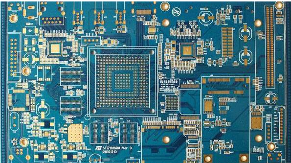
When laying out the PCBA circuit board, the first thing we need to consider is the size of the circuit board. If the size is relatively large, the printed lines are long, which will increase the resistance to resistance and reduce the ability to resist interference. If it is small, it will lead to poor heat dissipation of the circuit board, and adjacent lines are susceptible to interference. When determining the size of the circuit board, we need to determine the location of special components first, and finally we can eliminate the function of the circuit. To reasonably lay out the circuit board, generally follow the following rules.
1. It is necessary to shorten the connection between high-frequency components as much as possible, through this method to reduce the distribution parameters between them and the electromagnetic interference between each other, for those components that are easier to interfere, they cannot be close to each other. Too close, the input and output components should be as far apart as possible.
2. In view of the high potential difference between some components or wires on the PCB circuit board, the distance between them should be increased appropriately to avoid accidental short circuits caused by discharge. The components with high voltage should be arranged as far as possible in places that are not easily reachable by hands during debugging.
3. For components weighing more than 15g, they should be fixed with brackets and then welded. Those components that are large, heavy, and generate a lot of heat should not be installed on the printed circuit board, but should be installed on the chassis bottom plate of the whole machine, and the heat dissipation problem should be considered. Thermal components should be separated from heating components.

4. The layout of adjustable components such as potentiometers, adjustable inductors, variable capacitors, micro switches, etc. should consider the structural requirements of the whole machine. If it is adjusted inside the machine, it should be placed on the printed circuit board where it is convenient for adjustment; if it is adjusted outside the machine, its position should match the position of the adjustment knob on the chassis panel.
5. For devices with weak anti-noise ability and large power changes when turned off, such as RAM and ROM storage devices, the input and output capacitors should be directly connected between the power line and the ground line of the chip.
6. The power line design is based on the current of the printed circuit board, try to increase the width of the power line to reduce the loop resistance. At the same time, make the direction of the power line and the ground line consistent with the direction of data transmission, which helps to enhance the anti-noise ability.
7. The grounding wire should be as thick as possible. If the ground wire uses a very tight line, the ground potential changes with the change of the current, which reduces the anti-noise performance. Therefore, the ground wire should be thickened so that it can pass three times the allowable current on the printed board. If possible, the grounding wire should be 2~3mm or more.
How to carry out anti-interference of PCB circuit board needs to consider the problem from many aspects. The above introduction is only a brief introduction to some common anti-interference operations. In actual operation, what is needed is a combination of personal experience and function. To achieve anti-jamming operations.