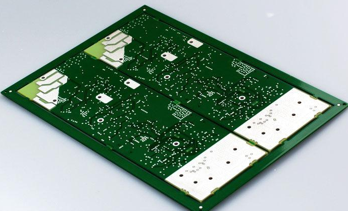
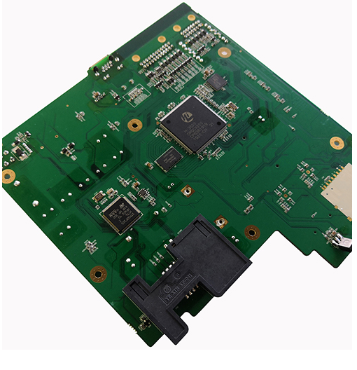
Operation rules of PCBA patch processing
The Internet era has broken the traditional marketing model, and a large number of resources have been gathered together to the greatest extent through the Internet, which has also accelerated the development speed of FPC flexible circuit boards, and then as the development speed accelerates, environmental problems will continue to appear in PCB factories. In front of him. However, with the development of the Internet, environmental protection and environmental informatization have also been developed by leaps and bounds. Environmental information data centers and green electronic procurement are gradually being applied to the actual production and operation fields.
1. There should not be any food or drink in the PCBA work area, smoking is prohibited, no sundries unrelated to work should be placed, and the workbench should be kept clean and tidy.
2. During PCBA patch processing, the surface to be soldered cannot be taken with bare hands or fingers, because the grease secreted by human hands will reduce solderability and easily lead to soldering defects.
3. The operation steps for PCBA and components are reduced to a minimum to prevent danger. In assembly areas where gloves must be used, soiled gloves will cause contamination, so gloves must be replaced frequently when necessary.
4. Do not use skin-protecting oils to coat hands or various silicone-containing detergents, as they can cause problems in solderability and adhesion of conformal coatings. A specially formulated detergent for PCBA soldering surface is available.

5. Components and PCBA that are sensitive to EOS/ESD must be marked with appropriate EOS/ESD marks to avoid confusion with other components. In addition, in order to prevent ESD and EOS from endangering sensitive components, all operations, assembly and testing must be completed on a workbench that can control static electricity.
6. Regularly check EOS/ESD workbenches to confirm that they can work normally (anti-static). The various dangers of EOS/ESD components can be caused by incorrect grounding methods or oxides in the ground connection parts. Therefore, special protection should be given to the "third line" grounding terminal joints.
7. It is forbidden to stack PCBA, otherwise physical damage will occur. There should be dedicated various brackets on the assembly work surface, and they should be placed according to the type.
In the PCBA patch processing, these operating rules should be strictly followed, and correct operation can ensure the final use quality of the product, and reduce the damage of the components and reduce the cost. iPCB is happy to be your business partner. Our business goal is to become the most professional prototyping PCB manufacturer in the world. With more than ten years of experience in this field, we are committed to meeting the needs of customers from different industries in terms of quality, delivery, cost-effectiveness and any other demanding requirements. As one of the most experienced PCB manufacturers and SMT assemblers in China, we are proud to be your best business partner and good friend in all aspects of your PCB needs. We strive to make your research and development work easy and worry-free.