The reliability of the PCB board manufacturers patch processing dip plug-in assembly is also the reliability of the PCB patch processing production process. It usually refers to the ability of the PCB board and PCBA board to not be damaged by normal operations during assembly and soldering. If the design is improper, it is easy to use Solder joints or components are damaged or damaged. Stress-sensitive devices such as BGA, chip capacitors, crystal oscillators are easily damaged by mechanical or thermal stress. Therefore, the design should be placed in a place where the PCB circuit board is not easily deformed. Or carry out reinforcement design, or adopt appropriate measures to avoid it.
(1) Stress-sensitive components should be placed as far away as possible from the bending during PCB assembly. For example, in order to eliminate the bending deformation during the assembly of the daughter board, the connector that connects the daughter board to the motherboard PCB factory should be connected as much as possible Place it on the edge of the daughter board, and the distance from the screws should not exceed 10mm.

For another example, in order to avoid BGA solder joint stress cracking, it is necessary to avoid BGA layout in the place where PCB assembly can be bent. The poor design of BGA can easily cause its solder joints to crack when holding the board with one hand.
(2) Reinforce the four corners of the large size BGA.
When the PCB is bent, the solder joints at the four corners of the BGA will be stressed and will be cracked or broken. Therefore, strengthening the four corners of the BGA is very effective to prevent the cracking of the corner solder joints. Special glue should be used for reinforcement. The use of PCBA patch glue for reinforcement requires space for component layout, and the reinforcement requirements and methods are indicated on the process documents.
The above two suggestions are mainly considered from the design aspect. On the other hand, the assembly process should be improved to reduce the generation of stress. For example, avoid holding the board with one hand and use support fixtures for mounting screws. Therefore, the design of assembly reliability should not only be Limited to the improvement of the layout of the components, the more important thing should be to reduce the stress of the assembly-adopt appropriate methods and tools, strengthen the training of personnel, and standardize the operation actions. Only in this way can the problem of solder joint failure in the assembly stage be solved.
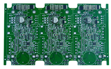
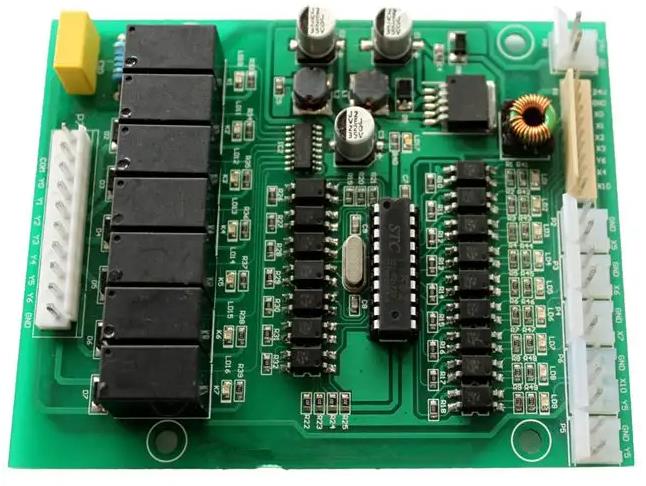
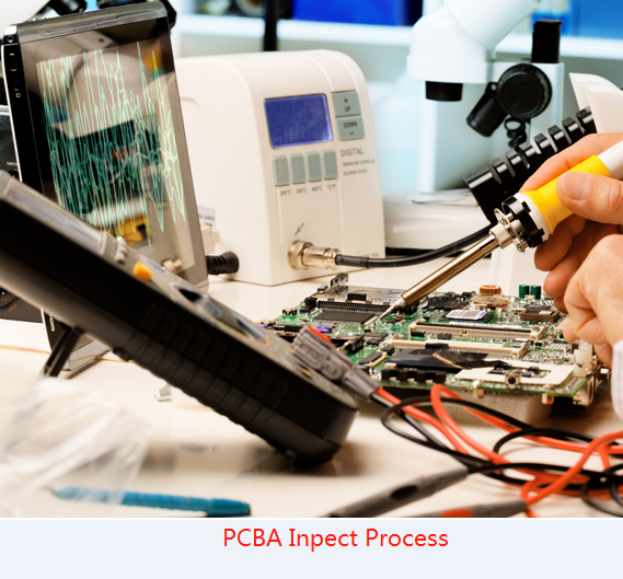
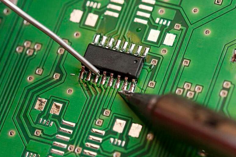
The soldering industry is the main process of PCB circuit boards in PCBA. This process is very important for PCBA, and everyone must pay special attention. In addition, PCBA soldering process has its own characteristics and processes, and it is the most basic according to the process. Only in this way can the effect be guaranteed. So, what are the basic processes and characteristics of the PCBA soldering process?
(1) The size and filling of the solder joints mainly depend on the design of the pad and the mounting gap between the hole and the lead. In other words, the size of the wave solder joint mainly depends on the design.
(2) The heat application of the PCB board manufacturer's patch processing of the PCB circuit board is mainly conducted by the molten solder. The amount of heat applied to the PCB circuit board mainly depends on the temperature of the molten solder and the contact time between the molten solder and the PCB circuit board (soldering Time) and area. Generally speaking, the heating temperature can be obtained by adjusting the transfer speed of the PCB board. However, the selection of the soldering contact area for the mask does not depend on the width of the wave nozzle, but on the tray window size. It is required that the layout of the components on the soldering surface of the mask should meet the requirements of the minimum opening size of the tray.
(3) The soldering chip type has a "masking effect", which is prone to solder leakage. The so-called "masking effect" refers to the phenomenon that the package body of the chip component prevents the solder wave from contacting the pad/soldering end.