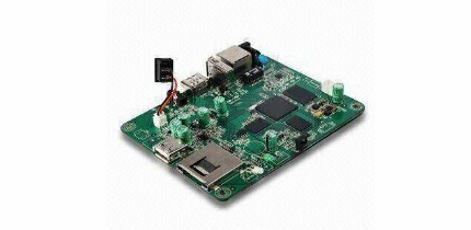
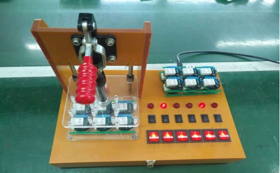
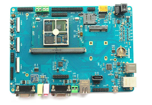
PCBA processing and production requirements
In the PCBA processing and production process, it is inevitable that there will be a series of equipment size or other requirements. What are the specific requirements? I will analyze and explain for you below.
1. PCB size background description
The size of the PCB is limited by the capacity of the production line equipment. Therefore, the appropriate PCB size should be considered when designing the product system scheme. In the following, Jingbang will explain this series of PCBA processing problems.
(1) The PCB size that can be mounted on SMT equipment comes from the standard size of PCB materials, most of which are 20" x 24", that is, 508mm x 610mm (rail width).
(2) The recommended size is the size that matches the equipment of the SMT production line, which is conducive to the production efficiency of each equipment and eliminates equipment bottlenecks.
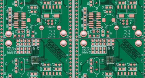
(3) For small-size PCBs, they should be designed as an imposition to improve the production efficiency of the entire production line.
PCB size design requirements
(1) Generally, the PCB size should be limited to 460mm x 610mm.

(2) The recommended size range is (200~250) mm x (250~350) mm, and the aspect ratio should be <2,
(3) For PCBs with a size of <125mm x 125mm, the appropriate size should be set up.
2. PCB shape background description
SMT production equipment uses guide rails to transport PCBs, and cannot transport PCBs with irregular shapes, especially PCBs with gaps in the corners.
PCB shape design requirements
(1) The shape of the PCB should be a regular square with rounded corners.
(2) In order to ensure the stability of the transmission process, the irregular shape of the PCB should be considered to be converted into a standardized square by means of imposition, especially the corner gaps should be filled in order to avoid jamming during the transmission of wave soldering jaws. plate.
(3) For pure SMT boards, gaps are allowed, but the gap size should be less than one-third of the length of the side where it is located. For those exceeding this requirement, the design process side should be filled.
(4) The chamfering design requirements of the golden finger. In addition to the chamfering design required by the figure when inserting the person, the two sides of the insert plate should also be designed with a chamfer of ((1~1.5) x 45 degrees to facilitate the insertion.
3. Background description of the transmission side
The size of the conveying edge depends on the requirements of the conveying guide rail of the equipment. For printing machines, placement machines and reflow soldering furnaces, the conveying edge is generally required to be 3.5mm or more.
Transmission side design requirements
(1) In order to reduce PCB deformation during soldering, for non-imposed PCBs, the long side direction is generally used as the transmission direction; for imposition, the long side direction should also be used as the transmission direction.
(2) Generally, the two sides of the PCB or imposition transmission direction are used as the transmission side, as shown in Figure 8-8, the small width of the transmission side is 5.0mm, and there should be no components or solder joints on the front and back of the transmission side.
(3) For non-transmission side, there is no restriction on SMT equipment, and a 2.5mm component forbidden area is reserved.
Four. Background description of positioning hole
Many processes such as imposition processing, assembly, and testing require accurate positioning of the PCB. Therefore, positioning holes are generally required to be designed.
Positioning hole design requirements
(1) For each PCB, at least two positioning holes should be designed, one is circular and the other is long groove shape, the former is used for positioning and the latter is used for guiding.
1. There is no special requirement for the positioning aperture, it can be designed according to the specifications of your own factory, and the recommended diameter is 2.4mm and 3.0mm.
2. The positioning holes should be non-metallized holes. If the PCB is a punched PCB, the positioning hole should be designed with a hole plate to strengthen the rigidity.
3. The length of the guide hole is generally 2 times the diameter.
4. The center of the positioning hole should be more than 5.0mm away from the transmitting edge, and the two positioning holes should be as far away as possible. It is recommended to arrange them at the opposite corners of the PCB.
(2) For mixed PCB (PCBA with plug-in installed), the position of the positioning hole is the same, so that the design of the tooling can be shared between the front and the back. For example, the screw base can also be used for the tray of the plug-in.
V. Background description of positioning symbols
Modern placement machines, printing machines, optical inspection equipment (AOI), solder paste inspection equipment (SPI), etc. all use optical positioning systems. Therefore, optical positioning symbols must be designed on the PCB.
(1) The positioning symbols are divided into global positioning symbols (Global Fiducial) and local positioning symbols (LocalFiducial). The former is used for the positioning of the whole board, and the latter is used for the positioning of imposition sub-boards or fine-pitch components.
(2) The optical positioning symbol can be designed into a square, diamond, circle, cross, tic-tac-toe, etc., with a height of 2.0mm. Generally, it is recommended to design a quasi-Omm round copper definition pattern. Taking into account the contrast between the material color and the environment, leave a non-soldering area 1mm larger than the optical positioning symbol, and no characters are allowed in it. The presence or absence of copper foil in the inner layer under the three symbols on the same board should be the same.
(3) On the PCB surface with SMD components. It is recommended to place three optical positioning symbols on the corners of the board for the three-dimensional positioning of the PCB (three points determine a plane, which can detect the thickness of the solder paste).
(4) For imposition, in addition to three optical positioning symbols for the entire board, two or three optical positioning symbols for imposition are also designed at the diagonal corners of each unit board.
(5) For devices such as QFP with lead center distance less than or equal to 0.5 mm and BGA with center distance less than or equal to 0.8 mm, local optical positioning symbols should be set at the diagonal corners for accurate positioning.
(6) If there are mounted components on both sides, there should be optical positioning symbols on each side.
(7) If there is no positioning hole on the PCB, the center of the optical positioning symbol should be more than 6.5mm away from the transmission edge of the PCB. If there is a positioning hole on the PCB, the center of the optical positioning symbol should be designed on the side of the positioning hole close to the center of the PCB.
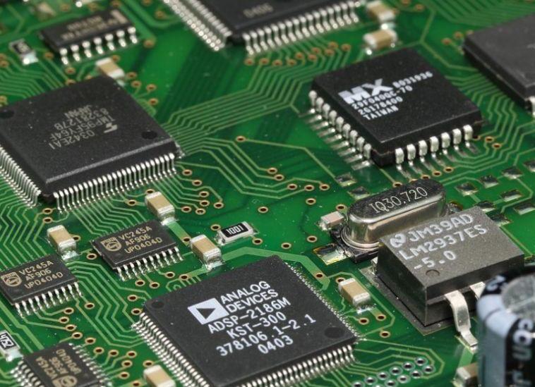
The difference between PCB and PCBA
What is PCB?
The Chinese name of PCB is printed circuit board, also known as printed circuit board. It is an important electronic component, a support for electronic components, and a carrier for electrical connection of electronic components. Because it is made by electronic printing, it is called a "printed" circuit board.
What is PCBA?
PCBA is the assembly of PCB. Various electronic devices are assembled on the circuit board through the surface packaging process. Next is the box assembly, which is about assembling the assembled PCB with the housing to form a finished product. That is to say, the blank PCB board goes through the SMT loading, and then goes through the entire manufacturing process of the DIP plug-in, referred to as PCBA. This is a common way of writing in China, while the standard way of writing in Europe and America is PCB'A, with an oblique dot added. PCBA is a PCB with a patch on it.
What is the difference between PCB and PCBA?
PCB refers to circuit board, and PCBA refers to circuit board plug-in assembly, SMT process.
One is a finished board and the other is a bare board
PCB (Printed Circuit Board) is called "printed circuit board" and is made of epoxy glass resin material. According to the number of signal layers, it is divided into 4, 6, and 8 layers. 4 and 6 layers are common. SMD components such as chips are pasted on the PCB.
PCBA may be understood as a finished circuit board, which means that PCBA can only be counted after the processes on the circuit board are completed.
PCBA=Printed Cirruit Board +Assembly.
That is to say, the empty PCB board goes through the SMT loading, and then goes through the entire manufacturing process of the DIP plug-in, referred to as PCBA.
PCB (Printed Circuie Board) is the abbreviation of printed circuit board, usually on the insulating material, according to the predetermined design, made into the conductive pattern of the printed circuit, the printed element or the combination of the two is called the printed circuit. The conductive pattern that provides electrical connections between components on an insulating substrate is called a printed circuit. In this way, the printed circuit or the finished board of the printed circuit is called a printed circuit board, also called a printed circuit board or a printed circuit board.