Recently, a friend asked what is a slot in the ground plane and its impact on PCB design. Next, PCB design company will introduce the slot in the ground plane.
Regarding the slots in the ground plane, the most important thing I can say is that they do not exist! If you have slots, no traces can cross them. If the trace does cross the slot, ask yourself this question: Where is the current return path? Remember the basic principle of EMC, "pass the smallest loop area possible, return current in a local and compact situation". If everyone follows this principle, many of our EMC problems will disappear or at least be minimized.
Slot in the ground plane
The lowest impedance signal return path is in the plane directly below the signal trace. The slots in the ground plane divert ground currents (see figure), resulting in high ground impedance (inductance) and ground plane voltage drops. This is the reason for the increased emissions of cables connected to the circuit board. In addition, the ground plane slots will significantly increase the crosstalk between the traces that span them, and the larger loop formed by the return current path will radiate.

A basic principle to reduce the noise radiation of high-speed signals on the PCB is to minimize the loop area of the current return path. The return current of high-speed signals is always biased towards the path with the lowest impedance, that is, the product plane next to the high-speed signal transmission line. The bottom is the GND ground plane, so when we make the via hole, we must pay attention to avoid the via hole breaking the ground plane to form a slot slot, which causes the signal return path area of the high-speed circuit to increase, increase noise radiation, and cause EMI problems.
The following table shows the measured value of the ground plane voltage with or without slot in the ground plane. The voltage measurement is made between two points on the ground plane, one inch apart and directly below the trace. As shown in the figure, the incision is cut perpendicular to the direction of the current and between the measurement points. The entrance under "Hole" represents a linear pattern of 15 holes, each with a diameter of 0.052 inches (perpendicular to the current flow), covering a linear distance of one inch. This represents an array of holes for the leads of through-holes or through-hole components. Use a 10 MHz, 3 nS rise time clock signal for voltage measurement, which flows down the trace and returns to the ground plane. It can be seen that the hole array does not increase the ground plane voltage
Afterwards, it is a difficult and time-consuming problem to find these problems on the buried ground plane that cannot be seen. However, there is a very simple way to initially check the quality of the ground plane. When you make a printed circuit board, you are required to engrave one set but not laminate. This way, you can view the unlaminated ground plane and quickly see if there is a problem. All new designs are a good practice.
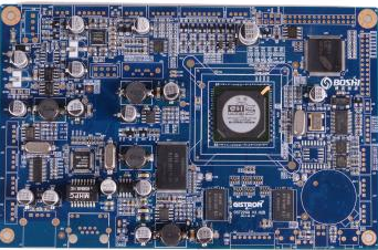
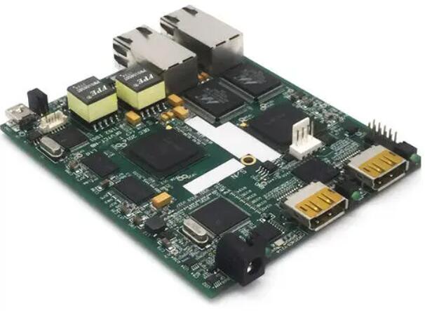
The above is the introduction of the slot in the PCB design ground plane. If you have circuit board products, you need to do PCB design,PCB manufacturing, component purchasing, SMT patch processing, DIP plug-in processing, PCBA foundry service, welcome Contact the PCB factory!