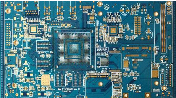
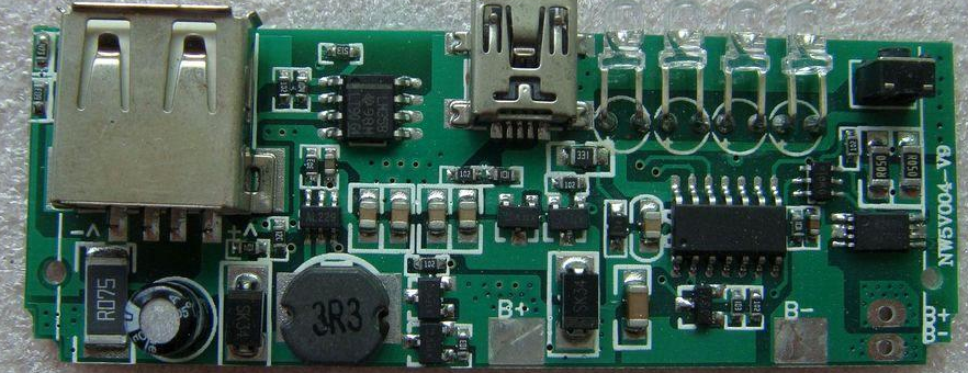
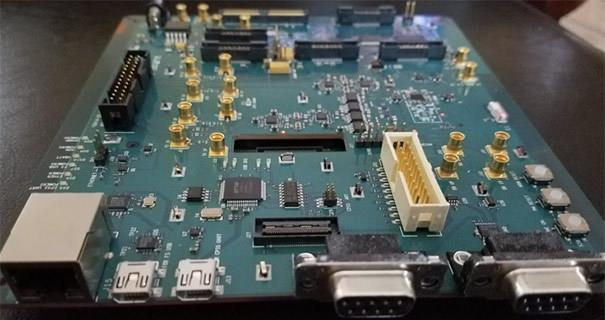
Shenzhen PCBA processing process
Paying attention to the trend of environmental protection informatization and the development of various environmental protection technologies, PCB factories can start with big data to monitor the company's pollution discharge and governance results, and find and solve environmental pollution problems in a timely manner. Keep up with the production concept of the new era, continuously improve resource utilization, and realize green production. Strive to make the PCB factory industry realize an efficient, economical and environmentally friendly production model, and actively respond to the country's environmental protection policy.
1. Printing solder paste
The squeegee pushes the solder paste forward along the surface of the template. When the solder paste reaches an opening area of the template, the downward pressure exerted by the squeegee forces the solder paste to pass through the opening area of the template and fall onto the PCB.
2. Apply adhesive

The PCB board with double-sided assembly is used to prevent the bottom surface mounting component during wave soldering or the bottom large integrated circuit component from melting and falling during double-sided reflow soldering, so the component needs to be stuck with an adhesive. In addition, sometimes in order to prevent the position of the heavier components from moving when the PCB board is transferred, it is also necessary to stick it with an adhesive.
3. Component placement
This process is to use an automated placement machine to pick up the surface mount components from the feeder and accurately mount them on the printed PCB board.
4. Inspection before and after welding
Before the components pass the reflow soldering, it is necessary to carefully check whether the components are well mounted and whether the position is offset or not. After the welding is completed, the solder joints and other quality defects need to be inspected before the components enter the next process step.
5. Reflow soldering
After the component is placed on the solder, the solder on the pad is melted by the flow soldering process of thermal convection technology to form the mechanical and electrical interconnection between the component lead and the pad.
6. Component insertion
For through-hole plug-in components and surface-mount components that cannot be mounted on certain machines, such as plug-in electrolytic capacitors, connectors, button switches, and metal terminal electrode components (MELF), perform manual insertion or use Automatic insertion equipment for component insertion.
7. Wave soldering
Wave soldering is mainly used to solder through-hole plug-in components. When the PCB board passes above the wave crest, the solder wets the leads leaking from the bottom surface of the PCB board, and the solder is sucked into the electroplating socket, forming a close interconnection between the component and the pad.
8. Cleaning
Optional process. When the solder paste contains organic ingredients such as rosin and lipids, the residues formed by combining them with water in the atmosphere after soldering are chemically corrosive, and leaving them on the PCB will hinder the reliability of the circuit connection., So these chemicals must be thoroughly cleaned away.
9. Maintenance
This is an off-line process whose purpose is to economically repair defective solder joints or replace defective components. Maintenance can basically be divided into three types: repair welding, heavy work and repair.
10. Electrical test
Electrical testing mainly includes online testing and functional testing. On-line testing checks whether the connection of each individual component and the test circuit is good; functional testing uses the working environment of the simulating circuit to determine whether the entire circuit can achieve a predetermined function.
11. Quality Management
Quality management includes quality control in the production line and product quality assurance before delivery to customers. It is mainly to check defective products, feedback the process control status of the products and ensure that the various quality indicators of the products meet the requirements of customers.
12. Packing and sampling inspection
The last step is to pack the components and conduct sampling inspections after packaging to again ensure the high quality of the products that will be delivered to customers. Pay attention to product innovation in terms of energy saving and emission reduction. PCB factoriesmust learn to attach importance to Internet technology and realize the practical application of automated monitoring and intelligent management in production through the integration of overall industry knowledge.