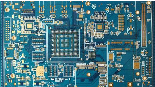
Issues that need attention in PCBA design
Schematic design before single-panel proofing is the preliminary work. When drawing the schematic, the hierarchical design should pay attention to the connection of each file into a whole at the end, which also has important significance for future work. Due to software differences, some software may appear to be connected but not actually connected (in terms of electrical performance). If you don’t use related testing tools, in case something goes wrong, it’s too late to find out when the board is ready. Therefore, Bai Qiancheng has repeatedly emphasized the importance of PCB production in order, hoping to attract everyone's attention.
The schematic diagram is based on the designed project. As long as the electrical connection is correct, there is nothing to say.
l. Make a physical frame
The closed physical frame is a basic platform for the future component layout and routing, and it also plays a constraining role for the automatic layout. Otherwise, the components coming from the schematic will be at a loss. But you must pay attention to accuracy here, otherwise installation problems in the future may be troublesome. In addition, it is best to use arcs at the corners. On the one hand, it can avoid sharp corners from scratching workers, and at the same time, it can reduce the effect of stress. In the past, one of my products always had the PCB board of the face shell broken during the transportation process, and it was just fine after using the arc.

2. The introduction of components and networks
It should be very simple to draw the components and the network in the good frame, but there are often problems here. You must carefully solve the errors one by one according to the prompts. Otherwise, it will take more effort. Generally speaking, the problems here are as follows: the package form of the component cannot be found, the component network problem, and there are unused components or pins. These problems can be solved quickly by comparing the prompts.
3. Layout of components
The layout and wiring of the components have a great impact on the life, stability, and electromagnetic compatibility of the product, so special attention should be paid. Generally speaking, there should be the following principles:
(1) Placement order
First place the components related to the structure at a fixed position, such as power sockets, indicator lights, switches, connectors, etc. After these components are placed, use the lock function of the software to lock them so that they will not be moved by mistake in the future. Then place special components and large components on the circuit, such as heating components, transformers, ICs, etc. Finally, place the small device.
(2) Pay attention to heat dissipation
Particular attention should be paid to heat dissipation in the component layout. For high-power circuits, the heating elements such as power tubes, transformers, etc. should be placed as close to the side as possible to facilitate heat dissipation. Do not concentrate in one place, and do not have high capacitors too close to avoid premature aging of the electrolyte. PCB circuit board proofing.
4. Wiring
Wiring principle: The knowledge of wiring is very advanced, everyone will have their own experience, but there are still some common principles.
5. Adjustment and perfection
After completing the wiring, all you need to do is to adjust the text, individual components, wiring, and apply copper (this work should not be too early, otherwise it will affect the speed and bring trouble to the wiring), also for the convenience of production, Commissioning and maintenance.
Copper coating usually refers to filling the blank area left by the wiring with a large area of copper foil. You can lay GND copper foil or VCC copper foil (but this way, it is easy to burn the device once a short circuit, so it is best to ground it, unless it is necessary to use it. To increase the conduction area of the power supply, to withstand a larger current before connecting to VCC). Grounding usually refers to wrapping a bunch of signal wires with special requirements with two ground wires (TRAC) to prevent them from being interfered by or interfered with by others.
If you use copper instead of the ground wire, you must pay attention to whether the entire ground is connected, the current size, flow direction, and whether there are special requirements to ensure that unnecessary errors are reduced.
6. Check the network
Sometimes the network relationship of the board drawn is different from the schematic diagram due to misoperation or negligence. At this time, it is necessary to check and verify. So don’t rush to hand it over to the plate maker after finishing the drawing, you should check it first, and then do the follow-up work.
7. Use simulation function for PCB circuit board proofing
After completing these tasks, software simulation can be carried out if time permits. Especially for high-frequency digital circuits, some problems can be found in advance, which greatly reduces the amount of debugging work in the future.