1. What are the general methods of PCBA proofing?
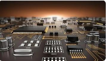
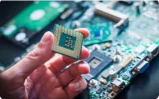
Nowadays, when you mention PCBA, I believe many people will feel a little strange to it. Because the field it needs to be applied to is relatively professional. And if we are involved in related aspects, it is better to take the initiative to pay attention to some knowledge related to it. In this regard, let's take a look at the general methods of PCBA proofing.
1. Direct proofing
The so-called direct proofing actually refers to applying a layer of photosensitive paste on the flat screen, wait until it is dry, and then use the relevant PCBA proofing film for effective bonding. But this method we must pay attention to is that in the process of coating, we must ensure that there are no stains, because in this way, the generation of bubbles can be well avoided.
1. Indirect proofing
If you choose to do PCBA proofing indirectly, you need to perform the exposure operation before proceeding with the production of the negative.

Generally, the film and the screen must be attached to each other when proofing, and then the film and the screen are tightly attached by squeezing. When necessary, it can be blown dry.
3. Straight proofing
The method of direct proofing is to first place the photosensitive film coated with photosensitive material on the work table with the photosensitive film facing up, and then wait for it to fully dry, then peel off the plastic base and attach the photosensitive film to the wrist. After the screen is developed and dried, a screen printing screen can be made.
2. What are the precautions for R&D model patch?
The research and development of sample patches is very good and can be completed in a relatively short time. It usually does not require additional material preparation. It can fully meet the sample patch needs of small and medium-sized enterprises that have started entrepreneurship. When developing sample patches, there are some The points to pay attention to, I will give you a specific introduction today.
1. In order to prevent the wrong placement of the R&D template patch, the number of bom must be analyzed first, and then the patch map is corresponding to the components with the same parameters, and the pictures are drawn with different colors.
2. In the process of R&D template placement, different components should be put in according to the different personnel. The personnel in the next process need to check the components and positions of the previous personnel's placement. If problems are found, they must be corrected in time., Finally, it is necessary to use the method of microscopy to check, and will cooperate with the use of a multimeter for measurement.
3. If the quality of the patch is controlled, it is usually operated by experienced professionals. The patch company has many full-time technicians and engineering and technical personnel. If there is a problem, it will be solved in time.
4. The soldering process of the R&D sample patch must be very secure. There are usually three more critical parts, such as solder paste printing, chip placement and furnace heating, etc. Each step must be ensured that there will be no problems. The people who put the chips in are all trained through many plates, and the whole process is very strict.
The process of R&D template mounting requires a series of steps to complete. When mounting, you must carefully operate and check carefully. If there are any problems, you must promptly inform professional technical personnel and give Timely correction processing, so as to obtain a relatively satisfactory R & D model patch.