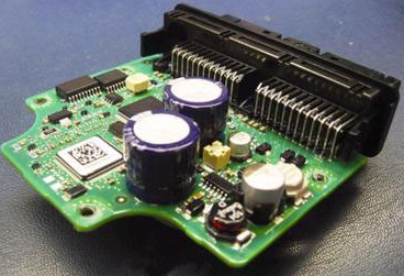
In the electronics production industry, we often use SMT patch processing, there are many common faults in the use process. According to statistics, 60% of patch failures come from solder paste printing. Therefore, ensuring the high quality of solder paste printing is an important prerequisite for the quality of SMT patch processing. The following explains how to solve printing failures in patch processing.
1. There is no gap between the stencil and PCB printing method, which is called "touch printing". It requires the stability of all structures and is suitable for printing high-precision solder paste. The stencil and printed board maintain a very smooth touch and are separated from the PCB after printing. Therefore, the printing accuracy of this method is relatively high, and it is especially suitable for fine-gap and super-macro solder paste printing.
1. Printing speed
With the push of the scraper, the solder paste rolls forward on the stencil. Fast printing speed is good for stencil
This kind of springback will also hinder the leakage of solder paste; and the speed is too slow, the paste will not roll on the stencil, resulting in poor resolution of the solder paste printed on the pad, usually with a finer printing speed.

2. Type of scraper:
There are two types of scrapers: plastic scrapers and steel scrapers. For ICs whose distance does not exceed 0.5mm, a steel squeegee should be used to facilitate the formation of solder paste after printing.
3. Printing method:
The most common printing methods are touch printing and non-contact printing. The printing method where there is a gap between the wire mesh printing and the printed circuit board is "non-contact printing." The void value is generally 0.5*1.0mm, which is suitable for solder pastes with different viscosities. The solder paste is pushed into the stencil by the squeegee, opening the hole and touching the PCB pad. After the scraper is gradually removed, the stencil is separated from the PCB board, which reduces the risk of vacuum leakage to the stencil.
4. Scratch adjustment
The squeegee operating point is printed along the 45° direction, which can significantly improve the unbalance of the different stencil openings of the solder paste, and can also reduce the damage to the thin stencil openings. The pressure of the squeegee is usually 30N/mm.
2. During installation, choose an IC mounting height with a spacing of no more than 0.5mm, 0 spacing, or 0~-0.1mm mounting height to prevent the solder paste from collapsing due to the low mounting height and short circuits during reflow.
Three, PCB remelting
The main reasons for assembly failure caused by reflow welding are as follows:
1. The heating speed is too fast;
2. The heating temperature is too high;
3. The heating speed of the solder paste is faster than the heating speed of the circuit board;
4. The flux gets too wet.
Therefore, when determining the PCB remelting parameters, all factors must be fully considered. Before batch assembly, ensure that the PCB soldering quality is not problematic before batch soldering.