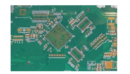
In PCBA processing, chip components often stand up, which is called tombstone. It is also called the suspension bridge and the Manhattan phenomenon. The same kind of welding defect, with so many names, shows that this kind of defect often occurs and attracts people's attention. The root cause of the tombstone phenomenon is that the wetting forces on both sides of the components are not balanced, so the moments at the two ends of the components are not balanced, which leads to the tombstone phenomenon.
In PCBA processing, chip components often stand up, which is called tombstone. It is also called the suspension bridge and the Manhattan phenomenon. The same kind of welding defect, with so many names, shows that this kind of defect often occurs and attracts people's attention.
The root cause of the tombstone phenomenon is that the wetting forces on both sides of the components are not balanced, so the moments at the two ends of the components are not balanced, which leads to the tombstone phenomenon.
The following situations will cause the imbalance of the wetting force on both sides of the component
1. Unreasonable pad design and layout

If one of the pads on both sides of the component is connected to the ground or the area of one side of the pad is too large, the uneven heat flux will cause the imbalance of the wetting force. The temperature difference across the PCB surface is too large to cause the component The heat absorption of the pad is uneven, large components QFP, BGA, and small chip components around the radiator also have uneven temperature.
Solution: Improve pad design and layout.
2. Solder paste and solder paste printing
The activity of the solder paste is not high or the solderability of the components is poor, and the surface tension of the tin is not the same after melting, which will also cause uneven wetting of the pad. The amount of solder paste printed on the two pads is uneven, and one side will absorb more heat due to the solder paste, and the melting time will lag, resulting in uneven wetting force.
Solution: Choose a solder paste with higher activity to improve the solder paste printing parameters, especially the window size of the template.
3. Patch
The uneven force in the Z direction will result in uneven depth of the components immersed in the solder paste. When melting, the wetting force on both sides will be uneven due to the time difference, and the displacement of the component patch will directly lead to the tombstone.
Solution: Adjust the parameters of the placement machine.
4. Furnace temperature curve
The PCB working curve is incorrect because the temperature difference on the board surface is too large. Usually, these defects will appear when the furnace body is too short and the temperature zone is too small.
Solution: Adjust the temperature curve according to each product.
A good working curve should be: the solder paste is fully melted; the thermal stress to the PCB components is the smallest; the various soldering defects are the lowest or no.
Usually at least three points should be measured
Soldering point temperature is 205 degree Celsius~220 degree Celsius;
The maximum PCB surface temperature is 240 degree Celsius;
The surface temperature of the components is less than 230 degree Celsius.