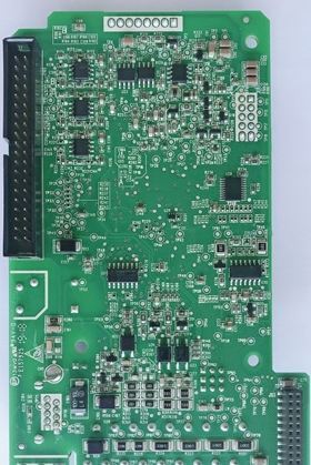
In the PCB processing and welding process, the performance of the flux directly affects the quality of the welding. So what are the common welding defects of PCBA processing? How to analyze and improve the bad welding?
1. Bad condition: There are too many residues on the PCB board surface after welding, and the board is dirty.
Result analysis:
(1) The temperature of the tin furnace is not enough because it is not preheated before welding or the preheating temperature is too low;
(2) The walking speed is too fast;
(3) Anti-oxidant and anti-oxidant oil are added to the tin liquid;
(4) Too much flux coating;
(5) The component feet and the orifice plate are out of proportion (the holes are too large), which causes the flux to accumulate;
(6) During the use of flux, no thinner is added for a long time.
2. Bad condition: easy to catch fire
Result analysis:
(1) The wave furnace itself has no air knife, which causes the flux to accumulate and drip onto the heating tube during heating;
(2) The angle of the air knife is incorrect (uneven flux distribution);

(3) There is too much glue on the PCB and the glue is ignited;
(4) The board travel speed is too fast (the flux is not completely volatilized and drips onto the heating tube) or too slow (the board surface is too hot);
(5) Process problems (pcb board, or PCB is too close to the heating tube).
3. Bad condition: Corrosion (green components, black solder joints)
Result analysis:
(1) Insufficient preheating causes too many flux residues and too many harmful residues;
(2) Use the flux that needs cleaning, but there is no cleaning after soldering.
4. Bad condition: electric connection, leakage (poor insulation)
Result analysis:
(1) PCB design is unreasonable
(2) PCB solder mask is of poor quality and easy to conduct electricity
5. Unfavorable phenomena: virtual welding, continuous welding, missing welding
Result analysis:
(1) The amount of flux coating is too small or uneven;
(2) Some pads or solder feet are seriously oxidized;
(3) PCB wiring is unreasonable;
(4) The foaming tube is clogged and the foaming is uneven, resulting in uneven flux coating;
(5) Improper operation method when immersing tin by hand;
(6) The inclination of the chain is unreasonable;
(7) The wave crest is uneven.
6. Bad phenomenon: the solder joints are too bright or the solder joints are not bright
Result analysis:
(1) This problem can be solved by choosing bright type or matte type flux;
(2) The solder used is not good.
7. Undesirable phenomena: smoke and smell
Result analysis:
(1) The problem of the flux itself: the use of ordinary resin will cause more smoke; the activator has a lot of smoke and has a pungent odor;
(2) The exhaust system is not perfect.
8. Unfavorable phenomena: splashing, tin beads
Result analysis:
(1) In terms of technology: low preheating temperature (the flux solvent is not completely volatilized); the board travel speed is fast, and the preheating effect is not reached; the inclination of the chain is not good, there are bubbles between the tin liquid and the PCB, and tin beads are generated after the bubbles burst; Improper operation during immersion tin; humid working environment;
(2) The problem of PCB: the board surface is wet and moisture is generated; the design of the outgassing hole of the PCB is unreasonable, resulting in air trapping between the PCB and the tin liquid; the design of the PCB is unreasonable, and the parts feet are too dense to cause air trapping.
9. Bad phenomenon: poor soldering, insufficient solder joints
Result analysis:
(1) The double wave process is used, and the effective components of the flux have been completely volatilized when the tin is passed;
(2) The board walking speed is too slow and the preheating temperature is too high;
(3) Uneven flux coating;
(4) The pads and component feet are seriously oxidized, causing poor tin eating;
(5) There is too little flux coating to completely wet the pads and component pins;
(6) The PCB design is unreasonable, which affects the soldering of some components.
10. Bad phenomenon: PCB solder mask falls off, peels off or blisters
Result analysis:
(1) More than 80% of the reasons are problems in the PCB manufacturing process: poor cleaning, poor quality solder mask, PCB board and solder mask mismatch, etc.;
(2) The temperature of tin liquid or preheating temperature is too high;
(3) Too many welding times;
(4) The PCB stays on the surface of the tin liquid for too long during the manual tin immersion operation.
The above is the bad welding phenomenon and result analysis in the PCBA processing.