This specification specifies the shape of the SMT steel mesh, the steel mesh logo, the materials used to make the steel mesh, and the process requirements for the opening of the steel mesh pad.
2. area
This specification applies to the design and production of steel mesh.
3 Responsibilities
Engineering Department: Responsible for the design of steel mesh openings.
4 Definition
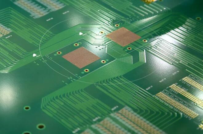
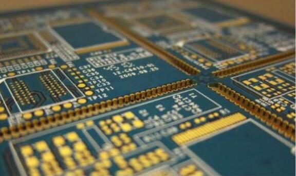
Stencil: also known as template, it is used to omit solder paste or glue in the SMT printing process
Flat mold.
MARK point: Optics designed to facilitate accurate alignment of the stencil and PCB during printing
location point
The material of the stencil frame can be a hollow aluminum frame or a solid aluminum frame, and the side length of the screen frame is
736736±5mm square, the thickness of the screen frame is 40±3mm. The bottom of the screen frame should be flat, and the uniformity should not exceed 1.5mm. The specifications of the external network frame are determined by the PE engineer and the external manufacturer.

Note: 550mm650mm steel mesh needs to have four fixing holes at the four corners of the frame: gauge
Grid size: 650550 Profile size: 4030, screw hole size: 4-M6, screw hole position: 600510, straight/hypotenuse: hypotenuse. The steel sheet material is preferably stainless steel, and its thickness is 0.08-0.3 (4- 12MIL). The wire mesh material is nylon wire, its mesh number should be no less than 90 mesh, and its minimum yield tension should not be less than 35N. The wire mesh material is stainless steel wire, its mesh number should be no less than 90, and its minimum yield tension should be No less than 35N. 5.1.4 The tape used for the net, the glue is on the bottom of the steel net, and the aluminum tape is used to cover the joint part of the steel sheet and the wire net and the part of the screen frame.
On the front side of the steel mesh, at the joint between the steel sheet and the wire mesh and the joint between the wire mesh and the screen frame, it must be filled with strong enough glue. The glue used should not be used with the cleaning solvent used for cleaning the steel mesh (industrial alcohol, xylene), Acetone, etc.) from a chemical reaction
a Generally, the method of laser cutting is adopted, and electropolishing is used after cutting to reduce the roughness of the hole wall.
b The glue stencil opening adopts the etching opening method.
c When the device spacing meets the following conditions, electroforming is recommended.
5.2.2 Stencil size (unit: mm) requirements: adhesive tape width C 20±5 20±5 stencil type screen frame size A steel sheet size B screen frame thickness D printable range standard steel mesh small steel mesh 736736± 5
550650±5 570570±5
530430±5 4040±3
4030±3 550 550±5
490390±5
When the PCB size exceeds the printable range, the outline size of the stencil should be negotiated with the supplier, and the stencil should be specially designed. The PCB center, the steel sheet center, and the stencil outer frame center must overlap, and the center distance of the three in the stencil production is the oldest The night value does not exceed 3mm. The axis of the PCB steel sheet and the outer frame of the steel mesh should be consistent in the same direction, and the angular deviation of any two axes should not exceed 2°. 5.2.4 The content and location requirements of the manufacturer's logo The manufacturer's logo should be located on the steel sheet T In the lower right corner of the face, there are no requirements for its font and text size, but its symbols are required to be clear and easy to distinguish, and its size should not exceed the rectangular area with a side length of 80mm40mm.
5.2.6 Stencil label content and location requirements
The stencil label needs to be affixed to the middle of the side of the stencil frame, as shown in Figure 1.
Stencil storage location and version number.
5.2.7 Requirements for the MARK point of the steel mesh
At least three MARK points must be made on the B side of the stencil, and the MARK points on the stencil and the printed board should be the same. If the PCB is a composite board, at least six MARK points must be made on the stencil. One-to-one correspondence with the PCB output side The MARK point on the upper side, the other pair corresponds to the pair of MARK points on the PCB with the farthest distance (on the non-auxiliary side).
5.3 Selection of steel sheet thickness
Under normal circumstances, the thickness of the steel sheet is selected according to the device with the smallest pin spacing on the PCB.
Decide
5.3.4 BGA repair ball planting small steel mesh
5.3.5 Selection principle of ladder steel mesh:
The stepped steel mesh is the same steel mesh, and the different pattern areas adopt different steel sheet thicknesses. When the PCB board has 0.4mm QFP, 0.5mmQFP, 0.5mmCSP/BGA, 0.8mmBGA and other fine-pitch devices, PLCC, and large surface mount transformers, Castle type devices, through-hole reflow soldering devices, and via-on pad devices coexist, you can choose a stepped steel mesh.
The ladder steel mesh includes upper ladder steel mesh and lower ladder steel mesh. The thickness of the ladder steel mesh is selected: the out part (C value) should not exceed the reference part by 0.05mm; consideration of the open ladder steel mesh: the size of the opening meets the volume ratio and area Ratio, the distance between the protruding part and the reference part device planning (A) and the distance between the opening of the protruding part and the edge (value B)