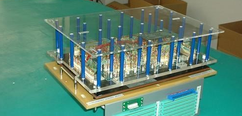
The following is an introduction to the precautions for PCBA making ICT fixtures:
1. Selection of test points:
1. Try to avoid placing needles on both sides of the fixture, and it is best to place the measured points on the same side.
2. The priority order of selected points to be tested (see Appendix A for details): Test point-DIP component pin-VIA via-SMT patch pin
2. Test points:
1. The center distance between the two measured points or the measured point and the pre-drilled hole is preferably not less than 0.050" (1.27mm). It is better to be greater than 0.100" (2.54mm), followed by 0.075" (1.905mm).
2. The measured point should be at least 0.100" away from the nearby parts (on the same side), if it is a part higher than 3m/m, the distance should be at least 0.120".
3. The measured points should be evenly distributed on the PCB surface to avoid local high density.
4. The diameter of the measured point should preferably be no less than 0.035" (0.9mm), if it is on the upper needle board, it should be no less than 0.040" (1.00mm).

5. A square shape is better (the measurable area is increased by 21% compared to a circular shape). The measured points less than 0.030" need to be added to correct the target.
6. Pad and Via of the tested point should not have solder mask.
7. The measured point should be at least 0.100" away from the edge of the board or folded edge.
8. Try to avoid placing the measured point on the SMT part, because the tin contact surface is too small and the parts are easily crushed.
9. Try to avoid using too long part feet (greater than 0.170" (4.3mm)) or too large aperture (greater than 1.5mm) as the measured point, which requires special treatment.
3. Positioning hole:
1. The PCB to be tested must have 2 or more positioning holes, and the holes should not be tinted, and the position is best to be on the opposite corner of the PCB.
2. The positioning hole is selected diagonally and the 2 holes with the farthest distance are the positioning holes.
3. The position tolerance between the measured point and the positioning hole should be +/-0.002".
4. The diameter of the tooling hole is preferably 0.125" (3.175mm), with a tolerance of "+0.002"/-0.001".
4. Other:
Attachment A. The order of consideration of the location of test points (each copper foil, regardless of its shape, needs at least one testable point):
1. The pins of ACI plug-in parts are prioritized as test points.
2. The exposed copper part of the copper foil (test PAD), it is best to be tinned.
3. Plug-in feet for vertical parts.
4. Through Hole, no Mask is allowed.
Attached B, test point diameter
1. Above 1mm, the best test results can be achieved with general probes.
2. If the thickness is less than 1mm, a more precise probe must be used to increase the manufacturing cost.
3. The distance between points is better than 2mm (center point to center point).
Attachment C. Requirements for double-sided PCB (focus on being able to make single-sided testing):
1. SMD surface wiring must have at least 1 through hole penetrated to the dip surface as a test point, and the dip surface is used for testing.
2. If the through hole requires a mask, consider laying the test pad beside the through hole.
3. If it can't be made into single-sided, use double-sided fixture to make it.
4. If the empty foot is within the allowable range, testability should be considered. When there is no test point, the point must be pulled.
5. Back Up Battery preferably has a Jumper, which can effectively isolate the circuit during ICT testing.