1. SMT steel mesh production method: laser engraving, electropolishing.
2. Steel plate thickness: pitch≤0.5mm steel plate selects 0.13mm; pitch>0.5mm steel plate thickness selects 0.15mm.
3. The thickness of the steel plate ≥0.15mm adopts anti-tin bead design to engrave.
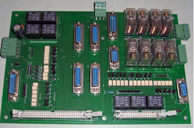
4. SMT steel mesh size: 650mm*550mm 420mm*520mm
5. Production accuracy: The steel plate opening error of 0402 components, BGA, QFP IC (0.5 mm pitch) is guaranteed to be within ±0.01 mm, and the component is guaranteed to be within ±0.02 mm.
6. MARK point production requirements: The production method is full engraving, and the minimum number of MARK points to be produced is 3.
7. Selection principle of MARK point:
7.1 If there are two MARK points on each of the two diagonals on the PCB circuit board, all four points must be carved out.
7.2 If there are only two MARK points on one diagonal, then another MARK point must be selected: the vertical distance to this diagonal is the farthest. (This point can be the QFP center point)
7.3 If other circumstances are involved, the stencil maker must be informed before production.
8. The principle of PCB component opening:

8.1 0805, 1206 steel mesh adopts 1:1 openings, 0805 opening spacing is 1.0mm, as shown in Figure 1: (using anti-tin beads). The 0603 opening is shown in Figure 2:
8.2 Glass diode open-hole pad expands outward anti-aircraft welding
SOT-23 package component opening method
8.3 SOT-23 packaged components should be reduced by 5%-10% at the time of opening.
8.4 The diameter of the opening during 1.27mm pitch BGA is 0.5mm-0.55mm, which is reduced by 5% on the basis of the pad.
8.5 1.00mm Pitch BGA pad opening 1:1.
8.6 QFP is greater than or equal to 0.5mm pitch, the opening is reduced by 10% on the basis of the pad and the corner is rounded (radius r=0.12mm).
8.7 Square diodes and tantalum capacitors: All holes are required to be engraved, and the inside and outside are expanded to ensure that there is a 0.5mm overlap between the component and the solder paste.
8.8 The width of 0.5mm pitch sop is 0.23mm, and the length is unchanged.
8.9 0.65mm pitch sop The cutting width is reduced by 10% to start cutting.
8.10 The opening area of SOT89 package components is reduced by 10%.
Open area of SOT89 package components
8.11 1206 pad mounts 0603 components. The engraved holes are centered on 0603 components, and the pad spacing is 0.70mm.
8.12 0805 pad paste 0603 component openings are centered according to the opening principle of 0603 components, and the pad spacing is 0.70mm.
8.13 The 1.2mm opening of the SOJ package IC can be equal to 95%. For the opening of the BGA diameter within 0.55mm:
8.14.1 0.55mm 8.14.2 0.5mm≤d≤0.55mm steel mesh opening diameter is 0.5mm. 8.14.3 The hole diameter of d<0.5mm steel plate is 0.46mm. For example: А 1.27mm pitch BGA / MPGA steel plate hole basic rules B 1.00mm pitch BGA / MPGA steel plate opening basic rules 8.15 The components and pads are engraved as shown in the figure when opening holes for non-polar capacitors of SMD above 1206: When opening a hole, only 2/3 of the PCB component solder feet are allowed to have solder paste, that is, the opening length = 2/3 component pins, and the width is 1:1 pad. 8.16 The pads of transistors and power transistors are large, and the pad spacing is small, and the anti-tin bead design should be adopted. The larger opening of one of the pins (as shown in the figure) uses a grid opening position at 2/3 of the circumference. 8.17 0402 (Unit: inch) The basic rules of chip steel plate opening: based on Gerber design, cut off an isosceles triangle at the four corners of the pad, and its waist length is 1/4 of the length of the PCB pad. 8.18 The design width of the resistance, capacitance and inductance of 0603 is 90% of the PCB pad length and the same length as the pad. Special cases deal with more short circuits. The length of the opening is consistent with the Gerber design size. The width of the opening: 0.35mm