The SMT chip factory can provide SMT chip processing services for the smallest package 0201 components, and supports various processing forms such as processing with materials and OEM materials. Next, I will introduce to you what inspections need to be done before SMT patch processing?
SMT chip processing
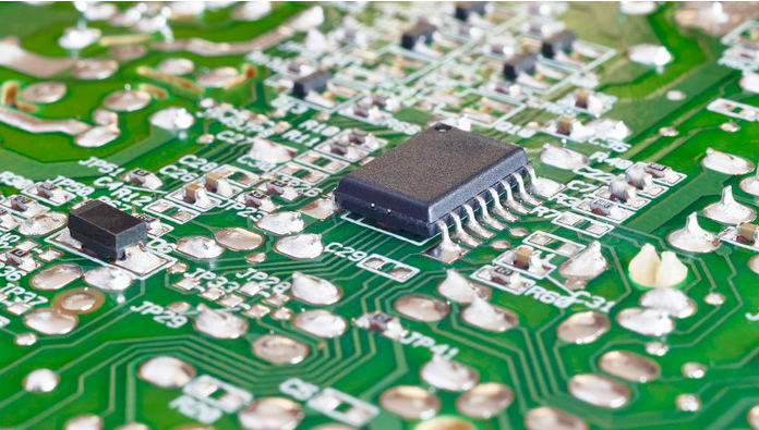
1. SMT component inspection
The main inspection items of components include: solderability, pin coplanarity and usability, which should be sampled by the inspection department. To test the solderability of components, stainless steel tweezers can hold the component body and immerse it in a tin pot at 235±5 degree Celsius or 230±5 degree Celsius, and take it out at 2±0.2s or 3±0.5s. Check the soldering end of the solder under a 20 times microscope, and it is required that more than 90% of the soldering end of the component is soldered.
SMT patch processing workshop can do the following visual inspections:
1. Visually or with a magnifying glass, check whether the solder ends or pin surfaces of the components are oxidized or have no contaminants.

2. The nominal value, specification, model, accuracy, and external dimensions of the components should be consistent with the product process requirements.
3. The pins of SOT and SOIC cannot be deformed. For multi-lead QFP devices with a lead pitch of less than 0.65mm, the pin coplanarity should be less than 0.1mm (which can be optically detected by the placement machine).
4. For products that require cleaning for SMT patch processing, the mark of the components will not fall off after cleaning, and will not affect the performance and reliability of the components (visual inspection after cleaning).
SMT processing incoming inspection
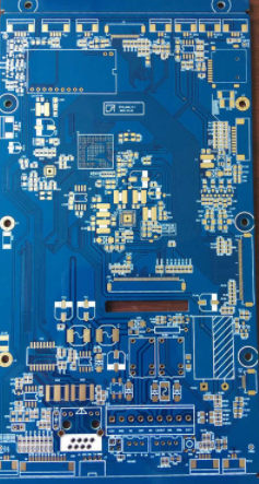
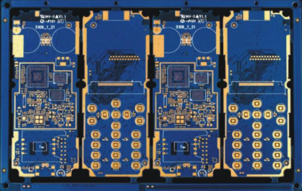
2. Printed circuit board (PCB) inspection
1. The PCB land pattern and size, solder mask, silk screen, and via hole settings should meet the design requirements of smt printed circuit boards. (Example: Check whether the pad spacing is reasonable, whether the screen is printed on the pad, whether the via is made on the pad, etc.).
2. The external dimensions of the PCB should be consistent, and the external dimensions, positioning holes, and reference marks of the PCB should meet the requirements of the production line equipment.
3. PCB allowable warpage size:
1) Upward/convex surface: maximum 0.2mm/5Omm length and maximum 0.5mm/the length direction of the whole PCB.
2) Downward/concave surface: maximum 0.2mm/5Omm length and maximum 1.5mm/the length of the whole PCB.
4. Check whether the PCB is contaminated or damp.
PCBA processing
Three, SMT patch processing matters needing attention
1. The SMT patch technician wears an OK-checked electrostatic ring, and checks that the electronic components of each order are free of errors/mixing, damage, deformation, scratches, etc. before plug-in.
2. The plug-in board of the circuit board needs to prepare the electronic materials in advance, and pay attention to the correct polarity of the capacitor.
3. After the smt printing operation is completed, check for defective products such as no missing insertion, reverse insertion, misalignment, etc., and flow the good tin finished products into the next process.
4. Please wear an electrostatic ring before SMT patch processing and assembly operations. The metal sheet should be close to the skin of your wrist and be well grounded. Work alternately with your hands.
5. Metal components such as USB/IF socket/shielding cover/tuner/network port terminal must wear finger cots when plugging in.
6. The position and direction of the inserted components must be correct, and the components must be flat against the board surface, and the elevated components must be inserted at the K foot position.
7. If any material is found to be inconsistent with the specifications on the SOP and BOM, it must be reported to the shift/group leader in time.
8. The materials should be handled with care. Do not drop the PCB board that has passed the previous process of smt and cause damage to the components. The crystal oscillator cannot be used if it is dropped.
9. Please tidy up the work surface before going to get off work and keep it clean.
10. Strictly abide by the operating rules of the work area. Products in the first inspection area, to-be-inspected area, defective area, maintenance area, and low-material area are strictly prohibited to be placed at will.