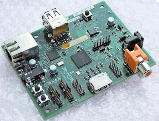
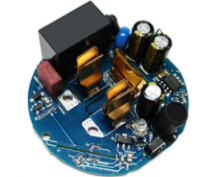
SMT chip processing reflow soldering causes voids
This article mainly introduces the causes of voids and cracks caused by SMT chip processing reflow soldering
It is inevitable that various bad phenomena will appear in the process of SMT patch processing. To solve these defects, we need to analyze the reasons for the undesirable phenomena. The reasons for voids and cracks caused by reflow soldering in SMT patch processing mainly include the following factors:
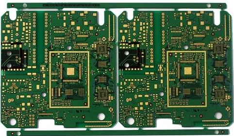
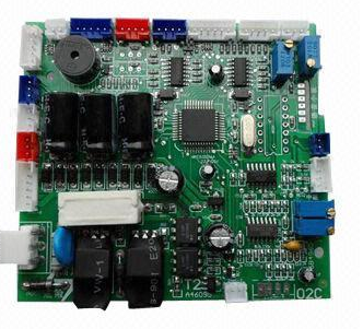
SMT chip processing reflow soldering causes voids and cracks
1. Poor penetration between PCB soldering board and component electrode.
2. The solder paste is not controlled as required.
3. The expansion coefficients of the welding and electrode materials do not match, and the solder joints are unstable during solidification.
4. The setting of the reflow soldering temperature curve cannot make the organic volatiles and water in the solder paste volatilize, and then enter the reflow area.

The problem with lead-free solder is high temperature, high surface tension and high viscosity. The increase in surface tension will inevitably make it more difficult for the gas to escape during the cooling stage, and it is difficult for the gas to escape, thus increasing the proportion of cavities. Therefore, in SMT chip processing, there will be more holes and voids in the lead-free solder joints.
In addition, since the temperature of SMT lead-free soldering is higher than that of leaded soldering, especially for large, multi-layer boards and components with high heat capacity, the peak temperature usually reaches about 260°C, and the temperature difference between the two is relatively large. Cool and solidify to room temperature. Therefore, the stress of lead-free solder joints is also higher. Coupled with more IMC, the thermal expansion coefficient of IMC is relatively large, and it is easy to crack under high temperature work or strong mechanical shock.
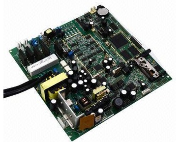
SMT chip processing reflow soldering causes voids and cracks
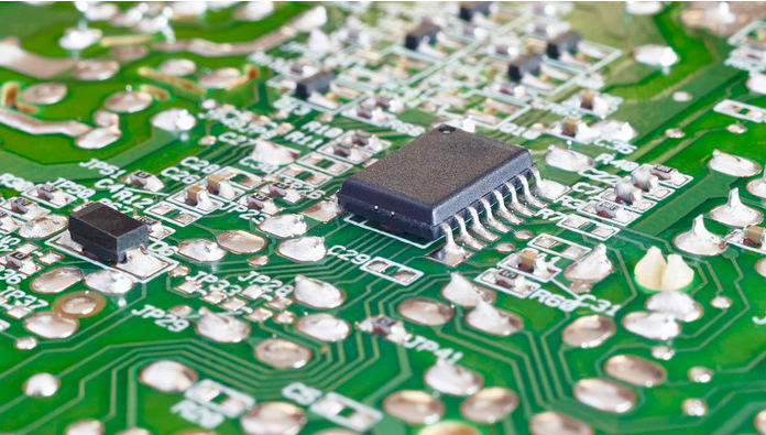
QFP, CHIP and BGA solder joint holes and the holes distributed in the solder interface will affect the connection strength of PCBA components. Solder joint cracks of SOJ pins, BGA ball and disc interface crack defects, solder joint cracks and solder interface cracks will all affect the long-term reliability of PCBA products.
The other is the hole or micro-hole at the weld interface. The holes are so small that they can only be seen with a scanning electron microscope (SEM). The location and distribution of the voids may be a potential cause of electrical connection failure. In particular, hollow measurement of power components will increase thermal resistance and cause malfunctions.
Studies have shown that the cavities (micropores) at the welding interface are mainly caused by the high solubility of copper. Due to the high melting point of lead-free solder and high-tin solder, the copper dissolution rate in SMT lead-free soldering is much higher than that in SN-PB soldering. The high solubility of copper in lead-free solder will form "holes" at the copper-solder interface, which over time may weaken the reliability of solder joints.