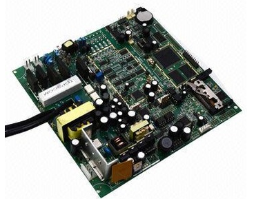
In order to ensure the quality of the appearance of SMT placement products, it is necessary to analyze and discuss the key elements in each link of production, and to formulate useful control methods for SMT placement processing. As a key process, solder paste printing is the most important thing. As long as the appropriate parameters are drawn up and the rules between them are grasped, high-quality solder paste printing quality can be obtained.
Skill control when applying solder paste
1. Before production, the operator uses special equipment to mix the solder paste to make it even, and it is best to use a viscosity tester or qualitatively to test the viscosity of the solder paste on time;
2. During the production process, 100% inspection of solder paste printing quality is carried out. The main content is whether the solder paste pattern is intact, whether the thickness is uniform, and whether there is a sharp appearance of the solder paste;
3. Strictly use the solder paste Longhua SMT chip processing within the useful life. The Suri solder paste should be stored in the refrigerator. It must be placed at room temperature for more than 6 hours before use, and then the cover can be opened and used. The used solder paste is stored alone. It is necessary to determine whether the quality is qualified when reusing;

4. After the printing test or printing failure, the solder paste on the printed board needs to be completely cleaned and dried with ultrasonic cleaning equipment to avoid solder balls after reflow caused by the residual solder paste on the board when used again;
5. After the first printing board is printed on duty or the equipment is adjusted on the same day, the solder paste thickness tester should be used to measure the thickness of the solder paste printing., The thickness of the solder paste is required to be between -10% and +15% of the thickness of the template;
6. Clean the template according to the skill requirements after the work on the shift is completed.
Metal content of solder paste
The content of the metal in the solder paste determines the thickness of the solder after soldering. With the increase of the percentage of metal content, the thickness of the solder for SMT patch processing is also increased. But at a given viscosity, with the addition of metal content, the bridging tendency of the solder increases accordingly.
After reflow soldering, the equipment pins are required to be welded firmly, with full solder volume, lubrication, and a 1/3 to 2/3 height climb in the direction of the end of the equipment (resistance container material). In order to satisfy the demand for the amount of solder paste in the solder joints, a solder paste with a metal content of 85% to 92% is generally selected. Solder paste manufacturers generally control the metal content at 89% or 90%, which has a very good application effect.
2. Common printing shortcomings and solutions for patch processing
Solder paste printing is a very messy skill. It is not only affected by data, but also directly related to equipment and parameters. After the control of each subtle link in the printing process, it can be said that the details determine the victory or defeat, in order to avoid printing The shortcomings that often appear in, the following is a brief analysis of the most common shortcomings that occur during solder paste printing and the corresponding avoidance or solutions.
1. The solder paste is too thin. The reason:
1. The template is too thin;
2. The scraper pressure is too large;
3. The solder paste has poor fluidity.
Avoidance or solution: choose a template with a suitable thickness; choose a solder paste with a suitable particle size and viscosity; reduce the pressure of the squeegee.
Second, draw the tip.
The sharpening is the solder paste on the pad after printing. The cause may be the gap of the squeegee or the viscosity of the solder paste is too high.
Avoidance or solution: SMT patch processing properly adjust the gap of the scraper or select a solder paste with a suitable viscosity.
3. After printing, the thickness of the solder paste on the pads is not the same, the reason:
1. The template is not parallel to the printed board;
2. The solder paste is not uniformly mixed, resulting in different particle sizes.
Avoidance or solution: adjust the relative position of the template and the printed board; mix the solder paste adequately before printing.
Fourth, fall. After printing, the solder paste sinks to both ends of the pad. The reason:
1. The scraper pressure is too large;
2. The positioning of the printed board is not firm;
3. The viscosity or metal content of the solder paste is too low.
Avoidance or solution: adjust the pressure; fix the printed board from the beginning; select the solder paste with suitable viscosity.
Five, the thickness is not the same. There are burrs on the edges and on the outside, which may be caused by the low viscosity of the solder paste and the rough wall of the template opening.
Avoidance or solution: choose a solder paste with a slightly higher viscosity; check the etching quality of the template opening before printing.
Sixth, the printing is not complete. Incomplete printing means that there is no solder paste printed on the PCB pads. The reason may be:
1. The opening is blocked or some solder paste sticks to the bottom of the template;
2. The viscosity of the solder paste is too small;
3. There are large-scale metal powder particles in the solder paste;
4. The scraper is worn.