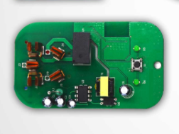
Chemically etched SMT patch processing template is the primary type of template international. They have the lowest cost and the fastest turnover. The chemically etched stainless steel template is manufactured by applying a corrosion protection agent on the metal foil, positioning the photosensitive object with a pin to expose the pattern on both sides of the metal foil, and then using the double-sided technology to corrode the metal foil from both sides. Because the technology is double-sided, the corrosive agent penetrates the holes, or openings, which occur in the metal, not only from the top and bottom surfaces, but also corrodes horizontally. The inherent characteristic of this skill is to form a blade, or hourglass shape. When the distance is below 0.020", this shape has a chance to stop the solder paste. This defect can be reduced by an enhanced technique called electropolishing.
A stepdown, or dual-level template, can be produced roughly through chemical etching techniques. This technique reduces the amount of tin in the selected components by forming downwardly stepped holes. For example, in the same characterization, a few 0.050"~0.025" spaced components (a template with a thickness of 0.007" is generally necessary) and a few QFP (quad flat pack) spaced 0.020" spaced together, in order to reduce the amount of solder paste in QFP, This 0.007" thickness template can produce a 0.005" thickness downward step area. The downward steps are usually on the scraper surface of the template, because the dry surface of the template must be on the entire board. Despite all this, it is recommended to provide at least 0.100" between the QFP and the surrounding components to allow the squeegee to completely distribute the solder paste in two levels of the template.

The chemically etched template is also optimal with regard to the half-etched fiducial and the title of the subtitle. The fiducial points used for the alignment of the printer's visual system can be half-etched and then filled with black resin to provide the visual system with a contrast with the lubricated metal scene that can be easily recognized by the visual system. The caption block including the part number, manufacturing date and other relevant information can also be half-etched on the SMT template for identification purposes. Both skills are completed by developing only half of the two sides.
Constraints of chemical etching. In addition to the defect of the blade edge, the chemically corroded template has another constraint: the aspect ratio. In short, this ratio constrains the smallest hole opening that can be etched according to the metal thickness at hand. Typically, for a chemically etched template, the aspect ratio is defined as 1.5:1. Thus, for a template with a thickness of 0.006", the smallest hole opening will be 0.009" (0.006"x1.5=0.009"). In contrast, for electroformed and laser-cut templates, the aspect ratio is 1:1, that is, 0.006" openings can be created on a template with a thickness of 0.006" by any technique.
Electropolishing is an electrolytic back-end technology that "polishing" the hole wall, resulting in reduced surface friction, excellent solder paste release, and general reduction. It can also greatly reduce the cleaning of the bottom surface of the template. Electropolishing is achieved by attaching a metal foil to the electrode and immersing it in an acid bath. The current causes the corrosive to corrode the rougher surface of the hole, and the effect on the hole wall is greater than the effect on the top and bottom surfaces of the metal foil, resulting in a "polishing" effect. Then, before the corrosive agent acts on the top and bottom surfaces, the metal foil is removed. In this way, the surface of the SMT hole wall is polished, so the solder paste will be effectively rolled (rather than pushed) on the surface of the template by the squeegee, and fill the hole.
Another technique for improving solder paste release for distances below 0.020" is trapezoidal section apertures (TSA).
Trapezoid face section (TSA) is an opening whose contact surface (or bottom surface) of the template is 0.001~0.002" larger than the size of the scraper surface (or top surface). Trapezoid face section can be completed in two ways: through selective retouching of special components, That is, the contact surface of the double-sided developing object is made larger than the scraper surface; perhaps all trapezoidal cross-section templates can be generated by changing the pressure settings of the top and bottom surfaces of the corrosive spray. After electropolishing, the hole The geometric shape of the wall allows the release of solder paste with a distance of less than 0.020". In addition, the resulting solder paste accumulation is a trapezoidal "brick" shape, which promotes stable placement of SMT components and fewer solder bridges.