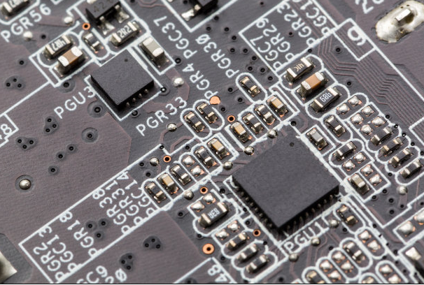
Manual visual inspection means that the operator’s eyes and rough optical zoom devices (magnifying glasses) conduct manual searches for the quality of circuit boards, dispensing, solder paste printing, PCB placement, PCB solder joints, and circuit board appearance. Using this method to conduct inspections, the initial investment is small, the craftsmanship is rough, but the craftsmanship is low, and it is impossible to search for small cracks in the appearance of solder joints and components, and the rest intensity is large, which will damage the eyesight of the inspection staff and is inappropriate. Consume a lot. After being lead-free, the details of the solder joints become rough and clumsy, showing a matt type, missing dazzling light and not conducive to visual inspection. However, the magnification of the component pins is a big trick for manual visual inspection, and it makes manual visual inspection more difficult. Therefore, this method is limited in the operation of most constrained consumption in this world.

1. Passive optical inspection (AOI inspection)
In order to meet the needs of high-density and fine-pitch assembly inspection, AOI inspection, that is, passive optical inspection, has become a serious skill in the SMT process. AOI inspection rejects the use of mobile phones, high-speed image processing, rewards and punishments, recognition of skills, and passive control. A detection technique composed of the integration of the skill, the prudential machine skill and the optical skill. It has a high degree of passivation, fast detection rate and high discrimination rate detection ability, which can reduce the intensity of rest, advance the accuracy of screening, reduce public fixtures, and have exquisite versatility, which can provide timely information to the assembly system.
2. Online circuit test (ICT test)
In the PCB line circuit test, namely ICT, there are two methods: flying probe and needle bed, and the outline drawing of the online circuit tester. The matter is to introduce the daisy chain topology layout when planning the chip and PCB board (the daisy chain topology is to use the shortest interconnection transmission line to connect all the devices, and each PCB device can only be adjacent to the other two via two transmission lines. On each device, until all the devices are adjacent, after the adjacency is realized, from the end of the first device, all the devices are adjacent to form a chain), so that the assembled solder joints form a network, so that the welding can be arbitrary through the on-off detection of the network. Can the point take effect. The detailed method is to use the probe to detect the electrical function parameters of the set point. Nowadays, single-head probes (spear type) are the most popular choice for consumers. They are generally used for inspection holes and pads. If they are used for pins, they will cause side slip: For the pins of through-hole PCB components, they will not be rejected. Needle type and powerful multi-faceted type. In order to improve the durability of the probe, if the probe material is selected from high-hardness steel, the detection pressure is generally in the range of 1-20N; and for no-wash solder paste, there is less flux waste, and the pressure range can be lower. Take 1.1~2.0N. The ICT test is also widely used after reflow soldering. It is mainly used to detect defects such as wrong polarity, bridging, false soldering, and short circuit of PCB components.