SMT process process 1, PCB board quality From each batch of goods or a specific batch number, take a sample to test its solderability. This PCB board will first be compared with the product data provided by the manufacturer and the PCB standard calibrated on the IPC. The next step is to print the solder paste on the solder pad and reflow. If organic flux is used, it needs to be cleaned to remove the residue. When evaluating the quality of solder joints, we should also evaluate the appearance and dimensions of the PCB board after re-soldering. The same inspection method can also be applied to the wave soldering process.

SMT process three: slim pitch skills Slim pitch assembly is a leading concept of construction and manufacturing. The component density and disorder are far greater than the mainstream products in the current market. If it is to enter the mass production period, it is necessary to modify some parameters before putting it into the production line.
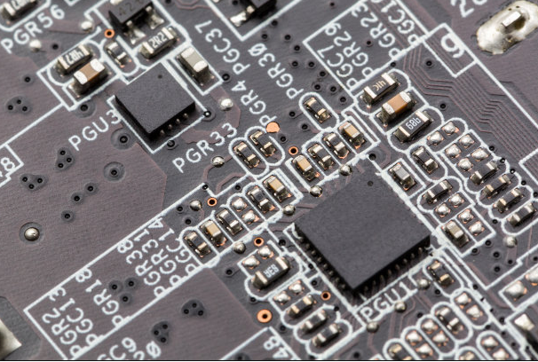
The dimensions and distance of the solder pads generally comply with the IPC-SM-782A standard. However, in order to meet the requirements of the manufacturing process, the shape and size of some solder pads will have a slight balance with this standard. For wave soldering, the pad size is generally slightly larger in order to have more flux and solder. For some components that are generally kept close to the upper and lower limits of the process tolerance, it is necessary to adjust the size of the solder pad appropriately.
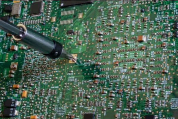
SMT process four: testing and repairing. Generally, it is appropriate, inaccurate and time-consuming to use small desktop testing tools to detect component or process defects. The testing method must be considered when describing. For example, if you want to use the ICT test, you must think about the online. When the full inspection is to inspect each product in a batch of products one by one, after picking out the unqualified products, it is considered that the rest are all qualified products. Although this quality inspection method is suitable for large-scale electromechanical equipment products with small production batches, most products with large production batches, such as electronic components products, are not suitable. When the product output is large, the inspection items are many or the inspection is more complicated, it will inevitably cost a lot of manpower and material resources to carry out the full inspection. At the same time, it is still inevitable that false inspections and missed inspections will occur. Describe some test points that the probe can touch. There are pre-written programs in the test system, which can test the function of each component, point out which component is faulty or incorrectly placed, and can distinguish whether the PCB solder joints are outstanding. The detection error should also include the short circuit between the component contacts, and the appearance of the empty solder between the pins and the solder pads. The ICT test is to manufacture different tools and test procedures without the need for the product. If the test is considered when describing the product, the product will be able to easily detect the quality of each component and PCB contact.