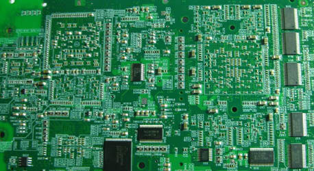
, Clean the PCB. Wipe the oil, dust, and oxide layer on the position, and then clean the wiping position with a brush or blow it off with an air gun.
, Die bonding glue. The amount of glue drops is moderate, the number of glue dots is 4, and the four corners are evenly distributed; the glue is strictly prohibited from contaminating the PCB pads.
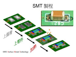
Chip paste (bonding). When using a vacuum suction pen, the suction nozzle must be flat to avoid scratching the surface of the wafer. Check the direction of the chip. When sticking to the PCB, it must be "smooth and positive": flat, the chip is parallel to the PCB, and there is no virtual position; stable, the chip and PCB are not easy to fall off during the whole process; positive, the chip and PCB reserved position are positive Paste, do not deflection, pay attention to the direction of the chip must not be reversed.
, Bangxian. Bonding PCB has passed the bonding tensile test: 1.0 line is greater than or equal to 3.5G, 1.25 line is greater than or equal to 4.5G. Standard aluminum wire with bonding melting point: the wire tail is greater than or equal to 0.3 times the wire diameter, and less than or equal to 1.5 times the wire diameter. The shape of the aluminum wire solder joint is oval. Solder joint length: greater than or equal to 1.5 times the wire diameter, and less than or equal to 5.0 times the wire diameter. The width of the solder joint: greater than or equal to 1.2 times the wire diameter, less than or equal to 3.0 times the wire diameter. The bonding process should be handled with care, and the points must be accurate. The operator should observe the bonding process with a microscope to see if there are any defects such as broken bonding, winding, deviation, cold and hot welding, aluminum lifting, etc., if any To notify the relevant technical personnel to solve the problem in time. Before the formal production, there must be a first-hand inspection to check whether there are any errors, few or missing states, etc. In the production process, there must be a dedicated person to check its correctness at regular intervals (up to 2 hours).

,test. Combination of multiple testing methods: manual visual inspection, automatic wire bonding quality inspection of bonding machine, automatic optical image analysis (AOI) X-ray analysis, inspection of the quality of inner solder joints
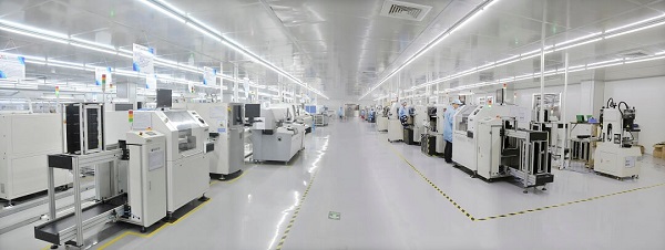
Standards for Bonding Processing and Loading Procedures
1. Check the PCB model and quantity. There must be no mistakes in this process.
2. Whether there is dust or oil on the surface of the PCB, if any, it should be cleaned before the board can be discharged. It must be strictly enforced to do a good job in the subsequent work.
3. The size of the red glue dots should not overflow the edge of the IC, and the IC sticking firmly is the standard. The IC sticking must be stable and regular. These all require careful and serious operation.
4. Check whether the IC is consistent with the PCB and record the batch number and date of the IC production; if the package has been opened, you must verify the quantity and check whether the IC is scratched. Any discrepancies found should be corrected in time.
5. Wear an anti-static ring, and use a negative pressure pen or a bamboo stick with double-sided tape to absorb the IC. It is strictly forbidden to scratch the surface of the IC or leave glue dots on the surface of the IC. Good quality requires a good working attitude.
6. Confirm whether the IC loading direction is correct and the angle is reasonable. After the first board is finished, the monitor should be checked. The first time this model is produced, it must be confirmed after bonding and testing Ok. Don't take it lightly.
7. The PCB aluminum boxes are stacked to 25 boxes per building, and they are neatly stacked and placed in the oven for drying. The processing efficiency is related to this.
8. The solidification temperature of red glue is 100-120 degree Celsius, and the drying time is 40-50 minutes. Operate strictly in accordance with the regulations.
9. Each board is accompanied by a "process sheet", which must be filled in carefully and truthfully, and flow into the next process together with the IC board. This is the most important manifestation of high efficiency and high energy.