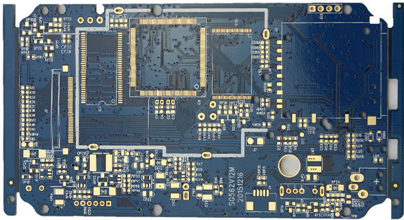
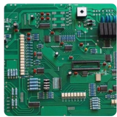
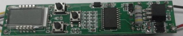
1.2.1 THC cartridge technology
1. Component lead forming
DIP devices need to reshape the pins before inserting
(1) Reshaping of components processed by manual SMT patch: the bent pin can be reshaped with the help of tweezers or a small screwdriver
2) Reshaping of machine-processed components: The machine reshaping of components is done by a special shaping machine. Its working principle is that the feeder uses vibration feeding to feed the material, (for example, the plug-in transistor) uses the divider to position the transistor. First The first step is to bend the left and right leads to form; the second step is to bend the middle lead back or forward to form.
2. Component insertion
Through hole insertion technology is divided into manual insertion and automatic mechanical equipment insertion

(1) For manual insertion and welding, the components that need to be mechanically fixed should be inserted first, such as the heat sink, bracket, clip, etc. of the power device, and then the components that need to be welded and fixed should be inserted. Do not touch the pins of the components and the copper foil on the printed board directly when inserting.
(2) Mechanical automatic plug-in (AI) is a more advanced automatic production technology in contemporary electronic product assembly. For automatic mechanical equipment insertion, the components with lower height should be inserted first, and then those with higher height should be installed. The valuable key components should be inserted at the end, such as heat sink, bracket, clip, etc. To be close to the welding process. PCB components assembly sequence
1.2.2 Wave soldering
(1) Working principle of wave soldering
Wave soldering is a process of forming a solder wave of a specific shape on the surface of the molten liquid solder with the help of pump pressure. When the assembly assembly with components inserted passes through the solder wave at a fixed angle, a solder joint is formed in the pin soldering area. technology. When the components are conveyed by the chain conveyor, they are first preheated in the preheating zone of the welding machine (the preheating of the components and the temperature to be reached are still controlled by the predetermined temperature curve). In actual welding, the preheating temperature of the component surface is usually controlled, so many devices have added corresponding temperature detection devices (such as infrared detectors). After preheating, the components enter the lead bath for soldering. The tin tank contains molten liquid solder, and the nozzle at the bottom of the steel tank sprays the molten solder out of wave crests of a fixed shape, so that when the component soldering surface passes through the wave, it is heated by the solder wave, and at the same time the solder wave wets the soldering area and proceeds. Expand the filling, and finally realize the welding process.
Wave soldering uses the principle of convection heat transfer to heat the soldering area. The molten solder wave acts as a heat source. On the one hand, it flows to wash away the lead pads, and on the other hand, it also plays a role of heat conduction, and the lead pads are heated under this action. In order to ensure the heating up of the soldering area, the solder wave usually has a certain width, so that when the soldering surface of the component passes through the wave, there is sufficient time for heating and wetting. In traditional wave soldering, a single wave is generally used, and the wave is relatively flat. With the use of lead solder, a double-wave form is currently adopted.
The pins of the components are solid, and the solder is immersed into the metallized through holes to provide a way. When the pin contacts the solder wave, with the help of surface tension, the liquid solder climbs up along the pin and the hole wall. Advances in the capillary action of metallized vias have promoted solder climbing. After the solder reaches the pad of the PcB part, it spreads out under the action of the surface tension of the pad. The rising solder exhausts the flux gas and air in the through hole, thereby filling the through hole, and finally forming a solder joint after cooling.
(2) The main components of the wave soldering machine
A wave soldering machine is mainly composed of conveyor belt, heater, tin tank, pump, flux foaming (or spraying) device, etc. Mainly divided into flux adding zone, preheating zone, welding zone and cooling zone.
1.2.3 The main difference between wave soldering and reflow soldering
The main difference between wave soldering and reflow soldering is the heating source and solder supply method in soldering. In wave soldering, the solder is pre-heated and melted in the tank, and the solder wave from the pump plays a dual role as a heat source and provides solder. The molten solder wave heats the through holes, pads and component pins of the PCB, and at the same time provides the required solder for the formation of solder joints. In reflow soldering, solder (solder paste) is pre-quantitatively distributed on the soldering area of the PCB, and the heat source during reflow is to remelt the solder.
1.3 Introduction to selective wave soldering process
Wave soldering equipment has been invented for more than 50 years. It has the advantages of high production efficiency and large output in the manufacture of through-hole components and circuit boards. Therefore, it was once the most important soldering equipment in the automated mass production of electronic products. However, there are certain limitations in its application:
(1) The welding parameters are different.
Different solder joints on the same circuit board have different characteristics (such as heat capacity, pin spacing, tin penetration requirements, etc.), and the required soldering parameters may be quite different. However, the characteristic of wave soldering is that all solder joints on the whole circuit board are soldered under the same set parameters. Therefore, different solder joints need to "combine" with each other, which makes it difficult for wave soldering to fully satisfy high-quality circuit boards. Welding requirements;
(2) Higher operating costs.
In the actual application of traditional wave soldering, the full-board spraying of flux and the generation of tin dross have brought higher operating costs; especially for lead-free soldering, because the price of lead-free solder is 3 times that of leaded solder As mentioned above, the increase in operating costs brought about by the generation of tin dross is very alarming. In addition, the lead-free solder continuously melts the copper on the pad, and the composition of the solder in the tin tank will change over time. This requires regular addition of pure tin and expensive silver to solve it;
(3) Maintenance and maintenance are troublesome.
The residual flux in the production will remain in the wave soldering transmission system, and the generated tin slag needs to be removed regularly, which brings more complicated equipment maintenance and maintenance work to the user;
For reasons such as this, selective wave soldering came into being.
The so-called PCBA selective wave soldering still uses the original tin furnace, the difference is that the board needs to be placed in a tin furnace carrier/tray (carrier), which is what we often call a furnace fixture.
Then expose the parts that need wave soldering to be tinned, and cover the other parts with a carrier for protection. It’s a bit like putting a lifebuoy in a swimming pool. The area covered by the lifebuoy will not get water. If you switch to a tin stove, the area covered by the carrier will naturally not get tin, and there will be no tin. Remelting tin or dropped parts.