1. The influence of halogen-free technology on smt patch processing
At present, many customers in the processing of smt will ask whether they can provide halogen-free technology. In simple terms, the halogen-free process means that the finished PCBA does not contain any elements in the 7th group of the periodic table. What are the specific 7th groups?
There is no doubt that the solder paste and flux that eliminates the halogen will have a large potential influence on the chip soldering process. The purpose of adding halogen to solder paste and flux is to provide stronger deoxidation ability, enhance wettability, and thus improve soldering effect. In combination with the current development of the enterprise industry in my country, it is in the middle of the lead-free transition of SMT patches, that is, we need to use different alloys with weak wettability (lead-free) and the original alloys containing lead solder.
In solder paste, the removal of halogens may negatively affect wettability and soldering. This will be a significant change in application, requiring a longer temperature curve or a very small area of solder paste deposition.
For example, 01005 welding requires a larger flux dose, and the absence of other halogen composite materials will more easily lead to "grape ball" defects. Two defects that can become very common during non-conversion are the "Head In Pillow" defect. This defect problem occurs due to the ability of BGA devices or PCB boards to deform easily during the reflow development process.

Since the BGA or substrate will separate the solder balls from the deposited solder paste when the BGA or substrate is bent, during the reflow stage, the solder paste and the solder balls melt, but do not contact each other, and an oxide layer is formed on the respective surfaces, so that they will re-open during the cooling process. When in contact, they are unlikely to bond together, causing the weld opening to look like a "pillow".
Because of the defects of the "grape ball" and "pillow" solder joints, the challenge for solder paste manufacturers is how to make the performance of the solderless paste as good as the company's current solder paste. Improving the performance of reflow is not so simple. Because the catalyst has been improved, it may have a negative impact on the solder paste printing process, template life and storage time. Therefore, when evaluating no material, the reflow performance and printing performance must be carefully tested. Effect.
Second, the direction of SMT equipment upgrade
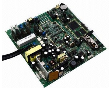
With the increasing miniaturization of electronic products and the increasing integration of IC, CPU, etc., the manufacturing industry urgently needs to transform and upgrade, and the design of electronic products is changing with each passing day. Intelligence and automation have become the trend of developing enterprises. Surface mount technology (SMT), as a new generation of electronic assembly technology, has developed rapidly in the past ten years. It has been widely used in various fields and has penetrated into various industries, and has partially or completely replaced traditional circuit board through-hole technology in many fields. This process can be roughly divided into: printing, SMT, welding and testing. With its own characteristics and advantages, SMT technology has made radical and revolutionary changes in electronic assembly technology. High-precision automatic printing, good SMT production is a process of SMT, SMT printing has a great influence on the pass rate of SMT products. One of the important factors that affect the quality of solder paste printing is the high accuracy of the motion control part of the printing machine. At present, SMT products are developing in the direction of high output and "zero defect". In production, the printing machine needs long-term stable and uninterrupted high-speed printing. Running speed, stability and reliability of the motion control system put forward very high requirements, and the innovative technology of printing component manufacturers continues to challenge the limits of production quality and production efficiency.
Focus on SMT full-line production, SMT placement machine has high performance and efficiency, high integration. The placement machine is used to realize high-speed, high-precision, and automatic placement of components. It is related to the accuracy and efficiency of the placement production line. The placement production line It is an investment of more than half of the entire production line with demanding equipment, key technology and stability, and the development trend of "three high-availability summary, four high-performance and efficiency, high integration, flexibility, intelligence, green, and diversification". With the miniaturization of electronic equipment, various high-function requirements, high-density and complex installation forms are higher than now, especially for the mixed installation of SMD and semiconductor.
High quality and green environmental protection, SMT reflow attaches importance to energy conservation and environmental protection. SMT reflow soldering is a soldering method preformed on the surface of the remelted solder. No additional solder is added during the soldering process. The heating circuit inside the device is blown to the After the components are attached to the circuit board, the air or nitrogen is heated to a high temperature, and the two sides of the solder components are bonded to the motherboard, which has become the mainstream technology of SMT. Through this process, most of the components on the circuit board are soldered to the circuit board. In recent years, the rise of various smart terminal devices has led to miniaturization of packaging and high-density assembly. Various new packaging technologies have become more advanced, and the quality of circuit assembly requirements has become higher and higher. Compared with manual inspection, automatic optical inspection, ICT test, functional test (FCT) and inspection methods,
X-RAY technology has more advantages and is widely used in SMT, LED, BGA, CSP flip chip inspection, semiconductor packaging components, lithium battery industry, electronic components, auto parts, photovoltaic industry aluminum, die-casting, molded plastic, Testing of ceramic products and other special dustries.