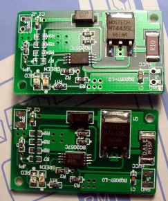
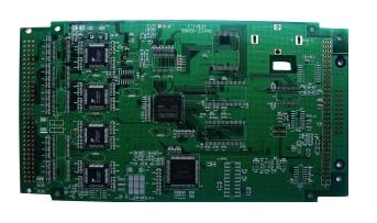
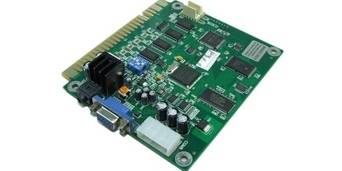
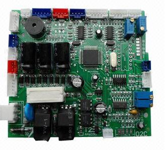
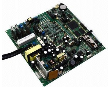
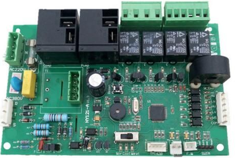
1. SMT patch processing quality inspection process
What are the quality inspection procedures for SMT patch processing? In order to connect SMT patch processing with one-time compliance rate and high reliability quality policy, it is necessary to design the printed circuit board scheme, electronic devices, materials, processing technology, machinery and equipment, The management system, etc. are manipulated. Among them, process management based on precautions is particularly important in the patch processing manufacturing industry. In each step of the entire process of patch processing, production, effective inspection methods must be followed to prevent various shortcomings and safety hazards before proceeding to the next process.
The quality inspection of patch processing includes quality inspection, processing technology inspection and surface assembly board inspection. Product quality problems discovered during the entire process of testing can be corrected in accordance with the repair status. The repair cost of unqualified products found in quality inspection, solder paste packaging printing and pre-welding grinding is relatively low, and the harm to the credibility of electronic equipment is relatively small.
But the repair of unqualified products after electric welding is different. As post-welding maintenance requires re-welding and welding from the beginning after desoldering, in addition to working hours and raw materials, electronic devices and circuit boards will also be destroyed.

According to the analysis of shortcomings, the whole process of quality inspection of SMT patch processing can reduce the failure rate, reduce the cost of repair and repair, and prevent quality damage from the root cause.
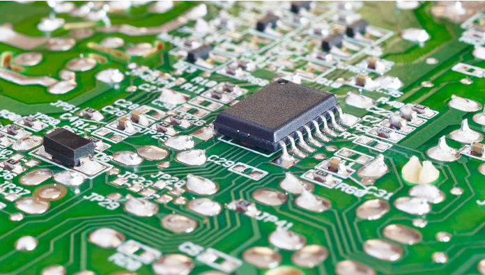
SMD processing and electric welding welding inspection are azimuth inspections of welded products. Generally, the points that need to be tested are: check whether the welding surface is smooth, whether there are holes, etc.; whether the welding is half-moon-shaped, whether there is more or less tin, whether there are defects such as tombstones, moving parts, missing parts, and tin beads. Whether each component has a different level of defects; check whether there are short-circuit faults, on-offs and other shortcomings during electric welding, and check the color change of the surface of the printed circuit board.
In the entire process of SMT chip processing, to ensure the quality of the electrical soldering of the PCB circuit board, it is necessary to pay attention to the effectiveness of the main parameters of the reflow oven processing process from beginning to end. If the basic parameters are not good, the welding quality of the printed circuit board cannot be guaranteed. Therefore, under all normal conditions, temperature control must be tested twice a day and ultra-low temperature test once. Only gradually improve the temperature profile of welded products and set the temperature profile of welded products to guarantee the quality of processed products.
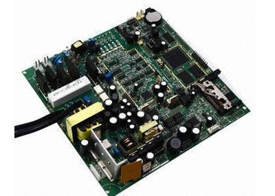
2. Desoldering skills in SMT chip processing
The main recommendation for disassembly of high pin density components in SMT patch processing is to use a hot air gun to clamp the components with tweezers, blow all the pins back and forth with the hot air gun, and lift the components when they are melted. If you need to disassemble the parts, do not blow to the center of the parts, and the time should be as short as possible. After removing the parts, clean the gasket with a soldering iron
1. For SMT components with a small number of pins, such as resistors, capacitors, bipolars and triodes, first tin plating on a pad on the PCB board, and then use tweezers to clamp the components in the mounting position with your left hand and fix them On the circuit board, use the right hand to solder the pins on the pads to the pads sold. The tweezers in the left hand can be loosened, and the remaining feet can be soldered with tin wires. This kind of part is also easy to disassemble, as long as both ends of the part and the soldering iron are heated at the same time, the tin is melted and lifted slightly to disassemble.
2. A similar method is used for chip components with a large number of needles and wide spacing. First, tin plating on the pad, then use tweezers to clamp the component on the left to solder one foot, and then solder the other foot with tin wire. It is usually better to disassemble these parts with a heat gun. On the other hand, the solder is melted by holding a hot air gun. On the other hand, when the solder is melted, parts are removed with a jig such as tweezers.
3. For the parts with high sales density, the welding technology is similar. First, solder the legs and use the wire to weld the remaining legs. The number of feet is large and dense, and the alignment of the nails and cushions is very important. Usually, the pads on the corners are plated with a small amount of tin, and the parts are aligned with the pads with tweezers or hands. The edges of the sale are aligned. These parts are pressed slightly harder on the printed circuit board, and the pins on the PCB pads are soldered with a soldering iron.