Friends in the patch processing industry know that solder paste plays a vital role in SMT patch processing, but how should solder paste be used? First of all, we must understand the storage method of tin, which can maximize the use of the solder paste, extend the service life of the solder paste, and save costs. Mastering the storage method of solder paste is beneficial to prolong the life of solder paste and can play its greatest role in use.
What is the solder paste printing for SMT chip processing?
First of all, the solder paste should be stored in the refrigerator. The storage temperature should be controlled within the range of 2 degree Celsius-10 degree Celsius. The service life of the unopened solder paste is 6 months, and the unopened solder paste is 24 hours. In a place where the sun can shine.
The solder paste of the SMT chip processing plant must be warmed up before use. The so-called warming is to put the solder paste at room temperature and let its temperature rise naturally to meet the requirements of use.

There are two purposes for the warming: It is used directly after reheating. The hot air outside will condense into water droplets on the surface of the solder paste, which will produce tin beads when passing through the reflow furnace. The viscosity of the solder paste is relatively high at low temperatures and cannot meet the printing requirements, so it can be used after reheating.
SMT patch processing plants pay attention to the shortest time the solder paste is opened, the better. After taking out enough solder paste on the same day, the inner cover should be covered immediately. Don't take a little bit and use a little bit during use. If you open the lid frequently, the solder paste will be in contact with the air for too long, which will easily cause the solder paste to oxidize.
After taking out the solder paste, close the inner cover immediately, press down forcefully to squeeze out all the air between the cover and the solder paste, so that the inner cover and the solder paste are in close contact. After confirming that the inner cover has been pressed tightly, screw on the large outer cover.
When the solder paste is no longer used, the remaining solder paste should be recycled into an empty bottle immediately. During the storage process, it should be kept completely isolated from the air. Never put the remaining solder paste into a bottle of unused solder paste. Therefore, in the process of taking solder paste, we should try to estimate the amount of solder paste as accurately as possible, and ensure that how much is used.
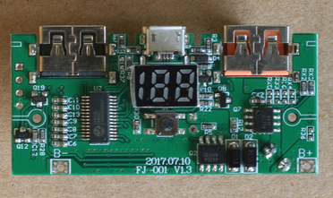
Inspection requirements for SMT patch processing products
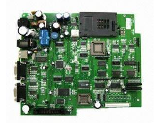
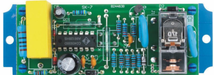
In the process of SMT chip processing products, the electronic products after the chip processing need to be inspected. What are the main points of the inspection? Let’s take a look at the following points:
1. Quality requirements of printing process
1. The position of the tin paste is in the middle, without obvious deviation, and can not affect the paste and soldering;
2. The printing tin paste is moderate, and it can be pasted well, and there is no less tin and too much tin paste;
3. The tin paste point is well formed, and there should be no continuous tin and uneven shape.
2. Quality requirements of component placement process
1. The component placement must be neat, centered, without offset or skew;
2. The type and specification of the components at the mounting position should be correct; the components should be free of missing or wrong pasting;
3., SMD components are not allowed to have reverse paste;
4. SMD devices with polarity requirements should be installed according to the correct polarity markings;
5. The component placement must be neat, centered, without offset or skew.
3. Component soldering process requirements
1. . The surface of the FPC board should be free of solder paste, foreign matter and marks that affect the appearance;
2. The bonding position of the components should be free of rosin or flux and foreign matter that affect the appearance and soldering tin
3. The tin spot under the components is well formed, and there is no abnormal wire drawing or sharpening.
4. Appearance process requirements of components
1. There should be no cracks or cuts on the bottom of the board, surface, copper foil, circuits, through holes, etc., and no short circuit caused by poor cutting;
2. The FPC board is parallel to the plane, and the board has no convex deformation;
3. . The FPC board should have no leakage V/V deviation;
4. . There is no blur, offset, reverse printing, printing deviation, ghosting, etc. in the silk-screened characters of the marked information;
5. There should be no swelling and blistering on the outer surface of the FPC board;
6. . The aperture size requirements meet the design requirements.