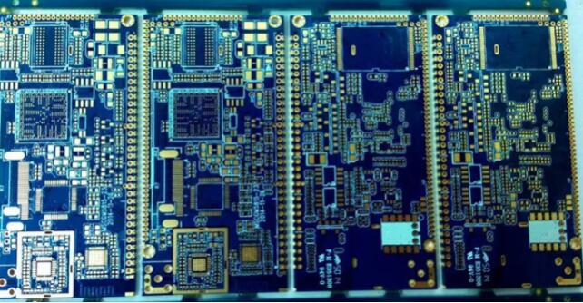
SMT chip processing solves the printing method of printing speed, printing method, type of scraper and scratch adjustment; in addition, it uses chip components with high reliability, small components and light weight, which has strong anti-vibration ability. Next, I will introduce the details for you
SMT chip processing solves the printing method of printing speed, printing method, type of scraper and scratch adjustment; in addition, it uses chip components with high reliability, small components and light weight, which has strong anti-vibration ability. Next, I will introduce the details for you.
1. How to solve printing in SMT patch processing
1. PCBA printing speed
With the push of the PCB scraper, the solder paste rolls forward on the stencil. Fast printing speed is conducive to the rebound of the stencil, and it will also hinder the leakage of solder paste; and the speed is too slow, the paste will not roll on the stencil, resulting in poor resolution of the solder paste printed on the pad. It is the interval where the printing speed is finer.

The scale bar is 10*20 mm/s.
2. PCBA printing method:
The most common printing methods are touch printing and non-contact printing. The printing method where there is a gap between the wire screen printing and the printed circuit board is "non-contact printing". The gap value is generally 0.5*1.0mm, which is suitable for different viscosities Solder paste. The solder paste is pushed into the stencil by the squeegee, opening the hole and touching the PCB pad. After the scraper is gradually removed, the stencil is separated from the PCB board, which reduces the risk of vacuum leakage to the stencil.
3. Type of scraper:
There are two types of scrapers: plastic scrapers and steel scrapers. For ICs whose distance does not exceed 0.5mm, a steel squeegee should be used to facilitate the formation of solder paste after printing.
4. Scratch adjustment
The squeegee operating point is printed along the 45° direction, which can significantly improve the unbalance of the different stencil openings of the solder paste, and can also reduce the damage to the thin stencil openings. The pressure of the squeegee is usually 30/mm.
Second, the advantages of SMT patch processing
1. High reliability and strong anti-vibration ability. SMT chip processing uses chip components with high reliability, small components and light weight, which has strong anti-vibration ability. It adopts automatic production and high installation reliability. Generally speaking, the defective solder joint rate is less than 10 parts per million, which is an order of magnitude lower than the wave soldering technology of the through-hole plug-in unit, which can ensure that the defective rate of the solder joints of electronic products or components is low. At present, nearly 90% of electronic products use s-MT technology.
2. Electronic products are small in size and high in assembly density
3. High-frequency characteristics and reliable performance. Because the chip components are firmly installed, lead-free or short leads are usually used, which reduces the influence of parasitic inductance and capacitance, improves the high-frequency characteristics of the circuit, and reduces electromagnetic and radio frequency interference. The higher frequency of the circuit designed by SMC and SMD is 3GHz, while the chip unit is only 500MHz, which can shorten the transmission delay time. It can be used in circuits with a clock frequency greater than 16mhz. If the MCM technology is adopted, the high-end clock frequency of the computer workstation can reach 100MHz, and the additional power consumption caused by parasitic reactance can be reduced by 2-3 times.
4. Improve production efficiency and realize automatic production. At present, in order to realize the complete automation of the perforated board, it is necessary to expand 40% of the original PCB area so that the plug-in head of the automatic plug-in can be inserted into the components, otherwise the space gap is not enough and the components will be damaged. The automatic sm421/sm411 adopts vacuum nozzle suction and exhaust parts. The vacuum nozzle is smaller than the component shape, but it increases the mounting density. In fact, small parts and small pitch QFPs are produced by automatic placement machines, realizing fully automatic production.
5. Reduce costs and expenses
(1) PCB area is 1/12 of the area of through-hole technology. If CSP is adopted, the area of PCB will be greatly reduced;
(2) Reduce the number of holes drilled on the PCB and save maintenance costs;
(3) Due to the improvement of frequency characteristics, the cost of circuit debugging is reduced;
(4) Due to the small size and light weight of PCB chip components, packaging, transportation and storage costs are reduced.