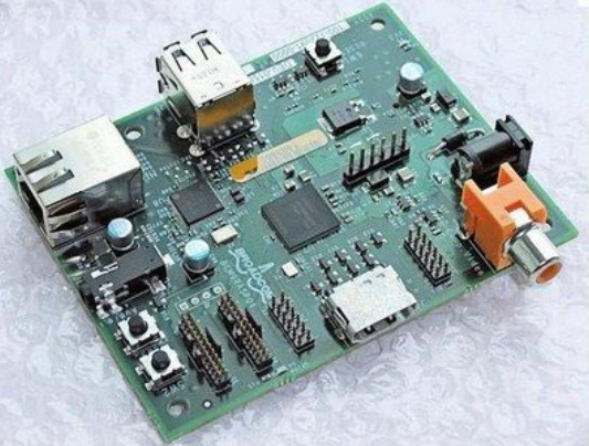
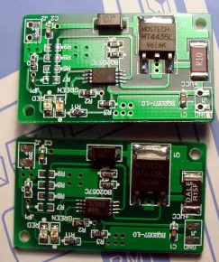
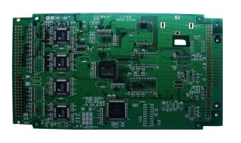
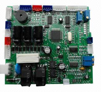
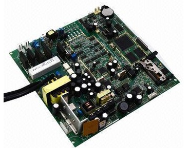
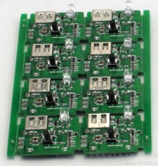
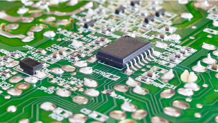
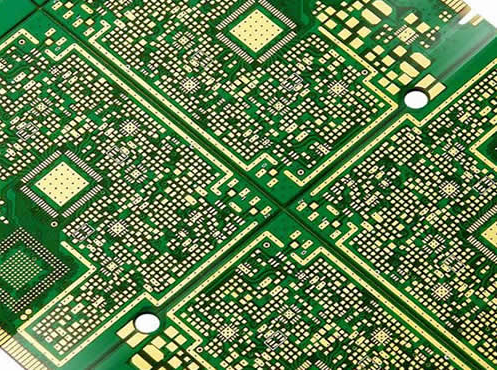
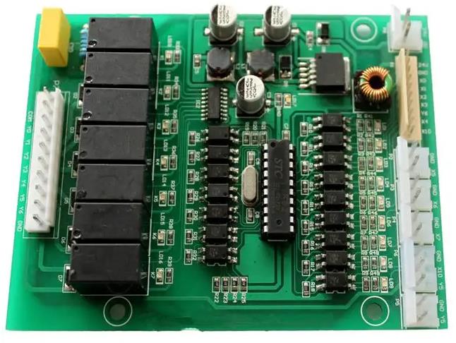
Surface mount technology (also known as SMT, Surface-mount technology) is an electronic assembly technology that originated in the 1960s. It was originally developed by IBM in the United States and gradually matured in the late 1980s. This technology is to mount electronic components, such as resistors, capacitors, transistors, integrated circuits, etc., on a printed circuit board, and form electrical connections by soldering. The components used are also referred to as surface-mount devices (SMD, surface-mount devices). The biggest difference from the through-hole insertion technology is that the surface mount technology does not need to reserve corresponding through holes for the pins of the components, and the component size of the surface mount technology is much smaller than that of the through-hole insertion technology. The overall processing speed can be increased by applying surface mount technology. However, due to the miniaturization of parts and the increase in density, the risk of circuit board defects increases. Therefore, in the circuit board manufacturing process of any surface mount technology, error detection has become A necessary part.

What are the advantages of SMT chip processing technology:
1. High reliability and strong anti-vibration ability
SMT chip processing uses chip components with high reliability. The components are small and light, so it has strong anti-vibration ability. It adopts automated production and has high mounting reliability. Generally, the rate of bad solder joints is less than 10 parts per million. The wave soldering technology of through-hole plug-in components is one order of magnitude lower, which can ensure a low defect rate of solder joints of electronic products or components. At present, almost 90% of electronic products adopt SMT technology.
2. Electronic products are small in size and high in assembly density
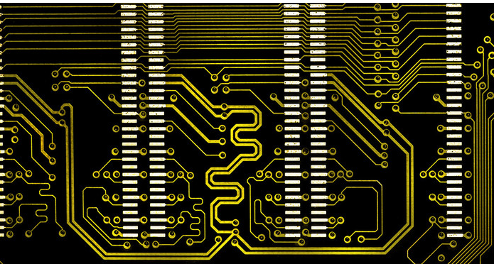
The volume of SMT chip components is only about 1/10 of the traditional plug-in components, and the weight is only 10% of the traditional plug-in components. Usually, the use of SMT technology can reduce the volume of electronic products by 40%~60% and the quality by 60%~80 %, the occupied area and weight are greatly reduced. The SMT patch processing assembly component grid has developed from 1.27MM to the current 0.63MM grid, and individual grids have reached 0.5MM. The through-hole mounting technology is used to install the components, which can make the assembly density higher.
3. Good high frequency characteristics and reliable performance
Because the chip components are firmly mounted, the devices are usually leadless or short leads, which reduces the influence of parasitic inductance and parasitic capacitance, improves the high-frequency characteristics of the circuit, and reduces electromagnetic and radio frequency interference. The maximum frequency of the circuit designed with SMC and SMD is 3GHz, while the chip component is only 500MHz, which can shorten the transmission delay time. It can be used in circuits with a clock frequency above 16MHz. If the MCM technology is used, the high-end clock frequency of the computer workstation can reach 100MHz, and the additional power consumption caused by parasitic reactance can be reduced by 2-3 times.
4. Improve productivity and realize automated production
At present, if the perforated printed board is to be fully automated, it is necessary to expand the area of the original printed board by 40%, so that the insertion head of the automatic plug-in can insert the components, otherwise there is not enough space and the parts will be damaged. The automatic placement machine (SM421/SM411) adopts a vacuum nozzle to suck and release the components. The vacuum nozzle is smaller than the shape of the component, which increases the installation density. In fact, small components and fine-pitch QFP devices are produced using automatic placement machines to achieve full-line automated production.
5. Reduce costs and reduce expenses
(1) The use area of the printed board is reduced, and the area is 1/12 of the through-hole technology. If the CSP is used for installation, its area will be greatly reduced;
(2) The number of drilling holes on the printed circuit board is reduced, saving repair costs;
(3) As the frequency characteristics are improved, the circuit debugging costs are reduced;
(4) Due to the small size and light weight of chip components, packaging, transportation and storage costs are reduced;
The use of SMT chip processing technology can save materials, energy, equipment, manpower, time, etc., and can reduce costs by 30% to 50%.