Nowadays, SMT chip processing technology has been more and more widely used in the electronics industry. In order to realize the miniaturization, thinner, lighter, and more functions of electronic products, the requirements for circuit board design are becoming more and more stringent, and the technical requirements are getting higher and higher.
Nowadays, SMT chip processing technology has been more and more widely used in the electronics industry. In order to realize the miniaturization, thinner, lighter, and more functions of electronic products, the requirements for circuit board design are becoming more and more stringent, and the technical requirements are getting higher and higher. Must have strict processing technology.
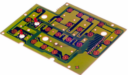
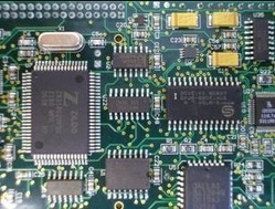
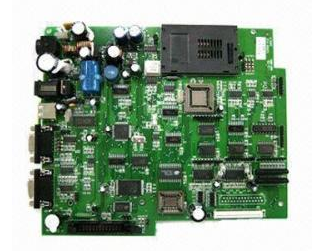
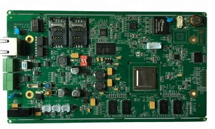
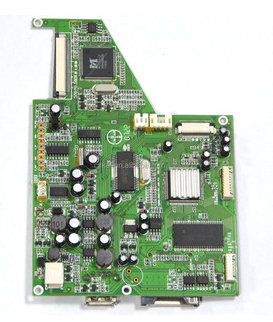
Introduction to the basic process of SMT patch processing
1. First of all, there must be a detailed patch location map before SMT patch processing, we need our Xingenyu electronics customers to provide samples, and design, develop and compile related programs based on the provided samples.
2. Before soldering the electronic components, the solder paste should be printed on the pad with a stencil. These need to be processed by a screen printing machine.
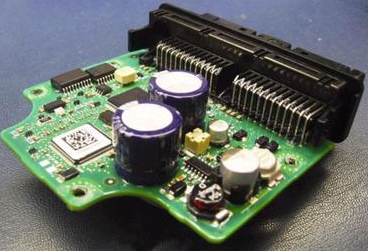
3. SMT patch processing in order to fix the electronic components on the PCB so that it is not easy to loosen, it must be glued on the fixed position of the PCB board.
4. Then use the placement machine to install the electronic components to be assembled on the PCB according to the position on the drawing.
5. Melt the patch glue on the PCB, so that the PCB board and the assembled electronic components are better glued together, and it is not easy to fall off with touch and shaking.
6. After the SMT chip is processed and soldered, a large amount of residue will be left on the PCB, which is harmful to the human body and affects the quality of the PCB. Therefore, it is necessary to remove them and use flux to remove them.

7. After completion, it is also necessary to check whether the assembly position is accurate, the quality after assembly, and whether it is qualified. Testing needs to be carried out with the help of magnifying glass, microscope, functional tester and other related measurement tools.
8. If a failure is found after SMT patch processing and inspection, rework, reorganization, and location inspection are also required.
Solutions to printing failures in SMT patch processing
In the electronics industry, SMT chip processing mostly uses SMT processing, and there are many common faults during use. According to statistics, 60% of defects are caused by solder paste printing.
In the electronics industry, SMT chip processing mostly uses SMT processing, and there are many common faults during use. According to statistics, 60% of defects are caused by solder paste printing. Therefore, ensuring the high quality of solder paste printing is an important prerequisite for the quality of SMT patch processing.
1. There is no gap between the stencil and the PCB printing method, that is, "touch printing". High stability requirements for all structures, suitable for printing high-precision solder paste. The metal screen is in good contact with the printed board, and is separated from the PCB after printing. Therefore, this method has high printing accuracy, and is especially suitable for fine-gap and super-macro printing.
1. Printing speed.
When the squeegee is pushed up, the solder paste rolls forward. Fast printing is good for stencils.
This kind of springback will also prevent the leakage of the solder paste, and the slurry cannot roll in the steel mesh, resulting in low resolution of the solder paste, which is the reason for the excessively fast printing speed.
The scale is 10*20mm/s.
2. Printing method:
Commonly used printing methods include touch printing and non-contact printing. The printing method for wire screen printing and printed circuit boards with blanks is "non-contact printing", which is generally 0.5*1.0mm, which is suitable for solder pastes of different viscosities. Use a scraper to push the solder paste into the stencil, open a hole and touch the PCB board. After the scraper is gradually removed, the stencil is separated from the PCB board, reducing the risk of vacuum leakage to the stencil.
3. Scraper type:
There are two types of scrapers: plastic scrapers and steel shovel. For ICs with a distance of no more than 0.5mm, steel solder paste can be selected to facilitate the formation of solder paste after printing.
4. Scraper adjustment.
In the welding process, the squeegee operating point is printed along the 45° direction, which can significantly improve the unevenness of the solder paste opening and reduce the damage to the thin steel plate with the opening. The pressure of the scraper is generally 30N/mm.
Solutions to printing failures in SMT patch processing
2. When installing, choose an IC mounting height with a spacing of no more than 0.5mm, 0mm, or 0~-0.1mm mounting height to avoid solder paste collapse due to too low mounting height and short circuit during reflow.
3. Remelting welding.
The main reasons for assembly failure caused by reflow welding are as follows:
a. Heating up too fast;
b. Overheating temperature;
c. The solder paste heating speed is faster than the circuit board heating speed;
d. The water flow is too large.
Therefore, when determining the remelting welding process parameters, all factors should be fully considered to ensure that there is no problem with the welding quality before mass assembly.