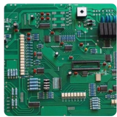
PCBA refers to the process of mounting, inserting and soldering bare PCB components. The production process of PCBA needs to go through a series of processes to complete the production. This article will introduce the various processes of PCBA production.
The PCBA production process can be divided into several major processes, SMT patch processing - DIP plug-in processing - PCBA testing - finished product assembly.
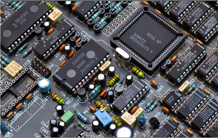
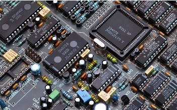
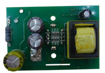
1. SMT patch processing link
SMT patch processing procedures are: solder paste mixing - solder paste printing - SPI - reflow soldering - AOI - repair
Solder paste mixing
After the solder paste is taken out of the refrigerator and thawed, it is stirred by hand or machine to suit printing and soldering
Solder paste printing
Place the solder paste on the stencil, and use a squeegee to print the solder paste onto the PCB soldering pad

SPI
SPI is the solder paste thickness detector, which can detect the printing of solder paste and control the effect of solder paste printing.
Placement
SMD components are placed on the feeder, and the placement machine head accurately mounts the components on the feeder on the PCB soldering pad through identification
Reflow soldering
The mounted PCB board is subjected to reflow soldering, through the high temperature inside, the paste-like solder paste is heated to become liquid, and finally cooled and solidified to complete the soldering
AOI
AOI is automatic optical inspection, which can detect the welding effect of PCB board by scanning, and can detect the defects of the board.
Repair
Repair the defects detected by AOI or manually
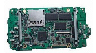
2. DIP plug-in processing link
The DIP plug-in processing procedure is: plug-in - wave soldering - cutting feet - post-welding processing - washing board - quality inspection
The plug-in processes the plug-in materials and inserts them on the PCB board
Wave soldering
The inserted board is subjected to wave soldering. In this process, liquid tin will be sprayed onto the PCB board, and finally cooled to complete the soldering
Cut feet
The pins of the soldered board are too long and need to be trimmed
After welding processing
Use an electric soldering iron to manually solder the components
Wash plate
After wave soldering, the board will be dirty, so you need to use washing water and washing tank to clean, or use a machine to clean
Quality inspection
Check the PCB board, unqualified products need to be repaired, and qualified products can enter the next process
Three, PCBA test
PCBA test can be divided into ICT test, FCT test, aging test, vibration test, etc.
PCBA test is a big test, according to different products, different customer requirements, the test methods used are different
The ICT test is to detect the welding of components and the on-off conditions of the circuit, while the FCT test is to detect the input and output parameters of the PCBA board to see if it meets the requirements.
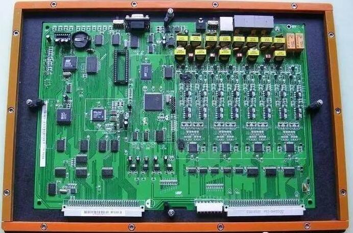
Fourth, finished product assembly
The PCBA board with the test OK is assembled for the shell, and then tested, and finally it can be shipped.