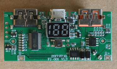
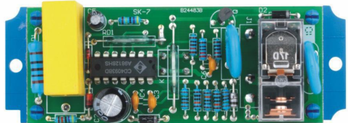
With the development of electronic products in the direction of small and thin, some electronic components with higher integration level and smaller pin spacing are more and more applied to PCBA motherboards, and the requirements for SMT chip processing are getting higher and higher., In order to ensure the welding quality of the product, it is necessary to strictly implement the technical standards of SMT patch.
SMT patch technical standards are:
1. SMT patch quality inspection standards
The SMT patch quality inspection standard is also known as the PCBA appearance inspection standard (IPC-A-610), as the global electronic assembly standard, the latest version is IPC-A-610F. The quality inspection standard defines the evaluation criteria and defects of welding quality and guides the PCBA processing process. It is the most basic quality inspection standard in electronic processing plants.
1. Definition of standards
2. Definition of defects
Two, SMT patch management specifications

The SMT patch process is more complicated, and any problem in any link will cause welding quality problems. Therefore, professional management standards are required in the processing process.
1. Comply with "Air Shower Regulations"
2. Factory 7S management
3. Standards for solder paste management
(1) Solder paste storage environment: refrigerating temperature 0 degree Celsius (2) When the new solder paste is put into the warehouse, check whether the outer packaging is damaged. After unpacking the outer packaging, check whether there is an ice bag inside the incubator package. Visually check whether the solder paste can is damaged, whether the solder paste package is sealed and stored, and whether it has been opened. (3) Check whether the manufacturer's model and quantity on the solder paste tank are consistent with the receipt, and the difference between the date of solder paste entering the factory and the validity period shall not be less than 6 months. (4) If there is any discrepancy in the inspection items, return it to the warehouse and notify the purchaser to contact the manufacturer for return processing! (5) After the solder paste inspection is qualified, the batch of solder paste is numbered, and the "Solder Paste Control Label" is pasted on the outer wall of the solder paste tank for tracking control during use! And fill in the "Solder Paste Storage Record Form" (6) For the placement of new solder paste, refer to the "Solder Paste Management Standards" to take out the last batch of solder paste, and store the new solder paste in the refrigerator in order according to the serial number. The placement principle: The numbering sequence is placed from right to left and from inside to outside. Finally, put the remaining solder paste from the previous batch on the outside. The principle of receiving solder paste: use the opened solder paste first, and check whether the solder paste is within the validity period. The use of new solder paste follows the principle of from left to right and from outside to inside (the number of solder paste bottles ranges from small to large). After the solder paste is taken out, fill in the temperature recovery date and time recorder on the "Solder Paste Control Label", etc. Related Information. (7) Requisition of solder paste: When the operator receives the solder paste, it is necessary to confirm whether the temperature of the solder paste meets four hours. Stir the solder paste. Stirring time: 5 minutes, 90% rotation speed. For the use of the solder paste mixer, refer to the "Specifications for the Use of Solder Paste Mixer" (8) When receiving solder paste, it is necessary to fill in the "Solder Paste Receiving Record Form" and the "Solder Paste Control Label". The service life of the solder paste is 24 hours. If it is not used up after 24 hours, it will be scrapped. Fill in the "Solder Paste Rejection Record Form" and have a technician or engineer sign it for confirmation. Three, SMT patch electrostatic management standards In the process of SMT patch processing, static electricity has always been an important factor causing chip damage. Due to the easy generation of static electricity, it is necessary to strictly manage static electricity in electronic processing plants to avoid unnecessary losses to electronic components. 1. Equipment grounding It is realized by connecting the metal wire with the grounding device, and the leakage current, static charge and lightning current that may be generated on the electrical equipment and other production equipment are introduced into the ground to avoid personal electric shock and possible fire accidents. 2. Wear electrostatic clothes, electrostatic shoes, and electrostatic bracelet; check that the electrostatic clothes and shoes pass the ESD test, and make a record. 3. Clean up all sources of static electricity in the work area, such as plastic bags, boxes, foam plastics or personal items (tea cups, hair clips, paper towels, key ornaments, glasses cases, etc.), and keep them at least 750px away from ESD sensitive components. Four, SMT patch cleaning standard When the PCB is printed with solder paste, if there are continuous tin, little tin, no tin, more tin, tin tip or stay on the production line for more than one hour, the PCB needs to be cleaned and reprinted. PCB cleaning steps: 1. Use a small scraper to scrape the solder paste on the PCB to the solder paste scrap box 2. Wet the dust-free wipe paper with plate washer water 3. Hold the PCB with your left hand, and wipe the surface of the PCB with a dust-free wipe with your right hand 4. After wiping, use an air gun to dry the PCB, and blow off the solder paste that is difficult to clean such as pinholes and screw holes Precautions: 1. The bad PCB must be cleaned within one hour 2. To clean the PCB in the cleaning area, separate the PCB to be cleaned from the cleaned PCB 3. Make sure that the pinholes, screw holes, etc. are cleaned. There are many SMT patch processing links, and a small factor can easily cause product defects. Only by implementing strict SMT patch technical standards can production be standardized and standardized, and product defects can be reduced.