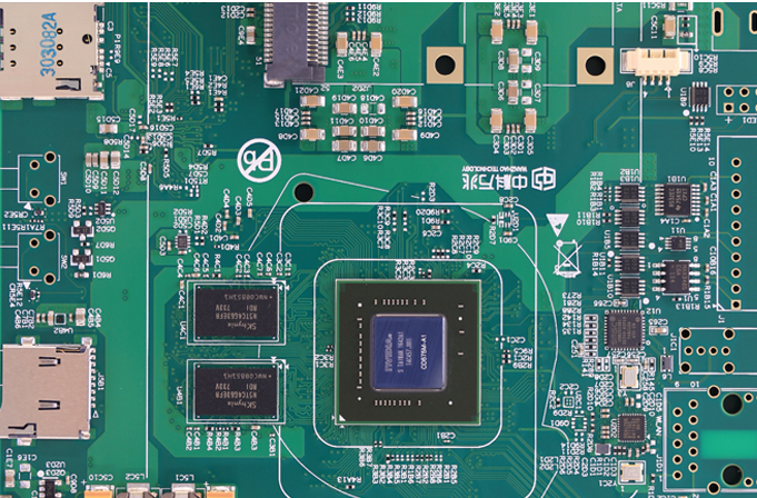
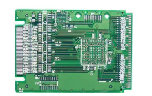
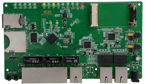
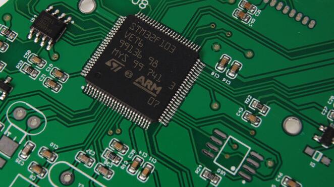
What is the PCBA board inspection project standard for SMT patch workshop? Here is an inventory of the PCBA board inspection items in the SMT patch workshop.
1. Empty welding of SMT parts
2. Cold welding of the solder joints of SMT parts: Use a toothpick to gently touch the pins of the parts.
3. SMT parts (solder point) short circuit (tin bridge)
4. SMT parts are missing
5. Wrong parts of SMT parts
6. The polarity of SMT parts is reversed or wrong, causing combustion or explosion
7. Multiple SMT parts
8. SMT parts overturning: the text side is facing down
9. SMT parts stand side by side: chip element length ≤ 3mm, width ≤ 1.5mm, no more than five (MI)

10. Tombstone of SMT parts: the end of the chip component is lifted
11. SMT parts foot offset: the side offset is less than or equal to 1/2 of the width of the weldable end
12. SMT parts floating height: the distance between the bottom of the component and the substrate <>
13. SMT parts foot high tilt: the height of the tilt is greater than the thickness of the part foot
14. The heel of SMT parts is not flat and the heel is not tinned
15. SMT parts cannot be identified (printing is blurred)
16. SMT parts foot or body oxidation
17. SMT parts body damage: capacitor damage (MA); resistance damage is less than 1/4 of the component width or thickness (MI); IC damage in any direction
18. SMT parts use non-designated suppliers: according to BOM, ECN
19. SMT parts solder point tin tip: the height of the tin tip is greater than the height of the part body
20. SMT parts eat too little tin: the minimum solder joint height is less than the solder thickness plus 25% of the height of the solderable end or the solder thickness plus 0.5mm, which is more
The smaller is (MA)
21. SMT parts eat too much tin: the maximum solder joint height exceeds the pad or climbs to the top of the solderable end of the metal plating end cap is acceptable, and the solder contact element
Piece body (MA)
22. Tin ball/tin dross: more than 5 solder balls or solder splash (0.13mm or smaller) per 600mm2 is (MA)
23. The solder joints have pinholes/blow holes: one solder joint has more than one (inclusive) as (MI)
24. Crystallization phenomenon: there are white residues on the surface of the PCB board, solder terminals or around the terminals, and white crystals on the metal surface
25. The surface of the board is unclean: the uncleanness that cannot be found within 30 seconds of a long arm distance is accepted.
26. Poor dispensing: the glue is located in the area to be welded, reducing the width of the end to be welded by more than 50%
27, PCB copper foil warped skin
28. PCB exposed copper: circuit (gold finger) exposed copper width greater than 0.5mm is (MA)
29. PCB scratches: no substrate is seen from scratches
30. PCB scorch: When the PCB is burnt and yellowed after the reflow oven or repaired, and the color of the PCB is different
31. PCB bending: the bending deformation in any direction per 300mm exceeds 1mm (300:1) is (MA)
32. PCB inner layer separation (bubble): the area where blistering and delamination does not exceed 25% (MI) of the distance between the plating holes or the inner wires;
Foaming between through holes or between internal wires (MA)
33. PCB with foreign matter: conductive (MA); non-conductive (MI)
34. PCB version error: according to BOM, ECN
35. Gold finger dip tin: the position of the tin dip is within 80% of the edge of the board (MA)