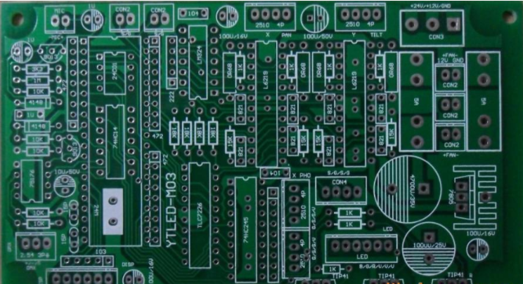
In the past few years, the wiping of the bottom of the steel mesh has attracted more and more interest. The changes in circuit design caused by miniaturized components and high-density interconnects have made it even more important to avoid any accumulation of solder paste on the steel mesh walls. Most smt stencil printing processes use vacuum dry wipe to clean the solder paste residue in the hole wall. The shrinking of the stencil aperture size requires more frequent wiping of the stencil to ensure that there is no accumulation of solder paste in the stencil.
In order to promote the release of solder paste, more and more researches are carried out around two technical methods. The first technology is nano-level hydrophobic, oleophobic and adhesion-reducing coatings. The method aims at nano-coating the surface of the metal steel mesh to prevent the solder paste from adhering to the hole wall. The second technique is to wet the stencil wipe cloth with a cleaning agent solvent to wipe the bottom. The cleaning agent dissolves the flux component in the solder paste, thereby promoting the release of the solder ball from the hole wall. Next, let's explain and analyze in detail.
1. Steel mesh release coating

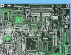
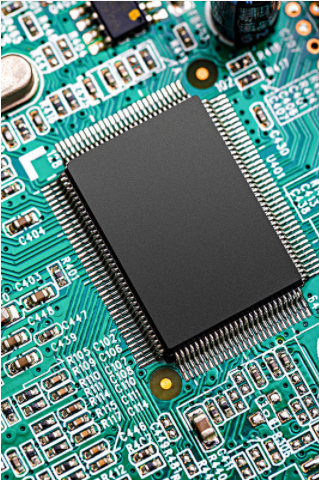
High-density and miniaturized circuit assembly make smt solder paste printing process challenges. The use of small components including 0201, 01005 and µBGA devices requires the use of high-quality solder paste to prevent solder paste bridging and misprinting. 2 The placement of these miniaturized components usually requires a higher forming ratio of solder paste release. In order to promote the release of solder paste, nano-coated steel mesh after laser cutting should be used to improve the transfer efficiency.
The nano-coating chemically changes the surface of the aperture to make the solder paste less attractive to the metal surface. The coated steel mesh works in two complementary ways to reduce the adhesion between the solder paste and the aperture. First, by adding a very thin coating to reduce the roughness of the pore size. And the coating fills some "recesses" of the surface structure. This process can reduce the adhesion of the solder paste to the stainless steel mesh wire.
The technology on which the nano-coated stencil relies is aimed at the ability to expel the solder paste from the openings. The ultra-thin oleophobic coating on the surface of the steel mesh verifies the improvement of fine-pitch printing and yield. The coating reacts with the surface of the steel mesh and the walls of the holes. The surface coating is about 5 monolayers thick. The coating changes the surface of the steel mesh through durable, hydrophobic, oleophobic and adhesion-reducing materials.
One problem has always been the frequency of scrubbing under the steel mesh. Many factors will affect the frequency of wiping. Generally speaking, in smt patch proofing or processing and production, miniaturized and high-density designs require more frequent scrubbing, because these designs make the excess solder paste more likely to deposit in the stencil aperture or stick after separation. Attached to the bottom surface of the steel mesh. The wiping frequency of highly miniaturized products can be one wiping per print, and the wiping frequency of low-density design can be one wiping every 10 to 20 prints.
For non-nano-coated steel mesh, pay attention to how the flux spreads on the bottom side of the steel mesh. The residual amount on the bottom side of the non-nano-coated steel mesh is very obvious.
The data found that if the stencil is nano-coated, the amount of solder paste and solder balls in the bottom side of the stencil and in the aperture is less. For high-level circuit design, nano-coating technology shows its advantages.
2. Wipe the solvent at the bottom of the steel mesh
For high-spacing structures, the underside of dry-wiping steel mesh has been approved. For large-scale printing jobs, a small amount of solder paste on the hole wall will not seriously affect the printing process. As the size of the structure decreases, it is usually necessary to use a chemical solvent to promote the dissolution of the flux carrier in the solder paste. The solder balls are released from the openings and released on the wiping cloth.
High-density PCB circuit boards and non-nano-coated steel mesh are used to study the effect of the wiping process underneath the steel mesh. Remove the stencil from the stencil printer after each printing. Check the aperture to observe the formation inside the aperture and the bottom side of the steel mesh.
For the formation of the bottom side of the steel mesh in multiple printing. As expected, the amount of solder balls and solder paste continues to increase during the printing process. The risk is that in the subsequent printing process, flux and excess solder balls will accumulate near the openings of the stencil. In addition to this, the small aperture is quickly blocked during the printing process.