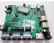
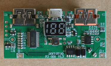
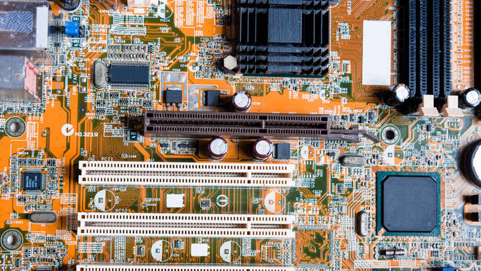
Everyone knows that with the continuous progress and development of technology, most electronic products nowadays are developed in small and medium-sized and light-weight. This also requires higher and higher requirements for PCB circuit boards. This is also based on SMT Only the chip processing technology can complete the lightness and miniaturization of the PCB. In SMT patch processing, solder joints are used as bridges for soldering. The quality and credibility of solder joints are also related to the quality of electronic products. So how do you distinguish the quality of solder joints during the production process? Xunde Electronic Stickers We will introduce the solder joint appearance inspection method of SMT chip processing in detail with everyone.
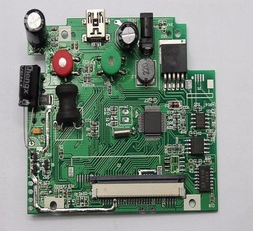
1. The solder joints and appearance of good SMT patch processing should meet the following points:
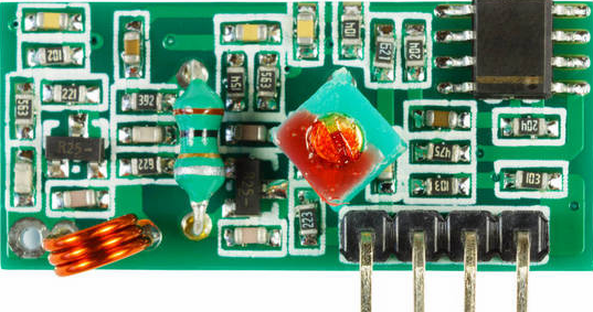
1. The surface of the solder joint should be complete, smooth and bright, without unevenness;
2. The wetting angle between the solder and the pad surface is preferably below 300, not more than 600.
3. The height of the component should be moderate, and the solder should completely cover the part where the pad and the lead are soldered
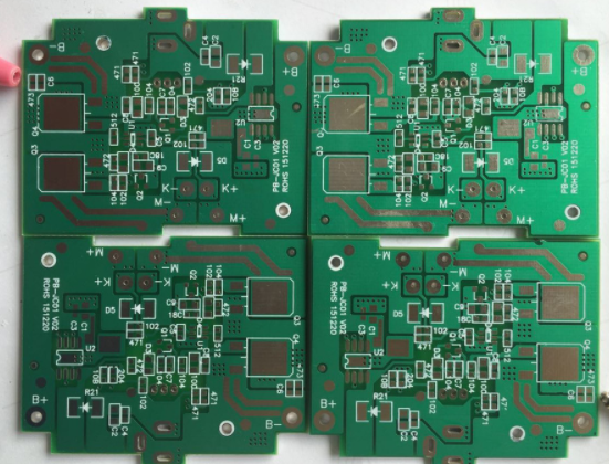
2. After SMT patch processing, PCB board inspection:
1. Are there any missing components?
2. Whether the component is mis-posted

3. Will it cause a short circuit?
4. Whether the component is soldered or not firmly
3. Visual inspection of solder joints
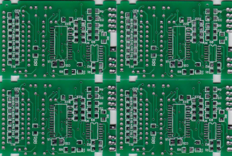
1. General components are inspected by AOI. The full name of AOI (Automated Optical Inspection) is automatic optical inspection. It is a device that detects common defects encountered in welding production based on optical principles. AOI is a new type of test technology that is emerging, but it is developing rapidly, and many manufacturers have introduced AOI test equipment. During automatic inspection, the machine automatically scans the PCB through the camera, collects images, compares the tested solder joints with the qualified parameters in the database, after image processing, checks out the defects on the PCB, and displays/marks the defects through the display or automatic signs Come out and be repaired by maintenance personnel.
Use high-speed and high-precision visual processing technology to automatically detect various mounting errors and soldering defects on the PCB board. PCB boards can range from fine-pitch high-density boards to low-density large-size boards, and online inspection solutions can be provided to improve production efficiency and welding quality. By using AOI as a tool to reduce defects, errors can be found and eliminated early in the assembly process to achieve good process control. Early detection of defects will avoid sending bad boards to the subsequent assembly stage. AOI will reduce repair costs and avoid scrapping unrepairable circuit boards.
2. X-ray (X-ray) detector for component inspection such as BDA uses low-energy X-rays without damaging the inspected item to quickly detect the inspected object.
The high-voltage impact target is used to generate X-ray penetration to detect the internal structure quality of electronic components, semiconductor packaging products, and the welding quality of various types of solder joints of SMT.