What is the meaning of SMT patch processing?
The meaning of SMT chip processing is to install and solder the required chip components to a fixed position on the printed circuit board. SMT means surface assembly technology, which is popular in the electronic processing industry. The materials for the SMT patch processing technology mainly include these contents: flux, solder paste, patch glue, etc. Solder paste is a kind of paste, used in the process of reflow soldering. Now SMT chip processing factories apply solder paste, the main method used is the stencil omission printing method. The advantage of this method is that it is easy to operate, but the reliability is unstable and the cost is high.
The patch glue is cured after being heated, and the solidification temperature is 150 degrees. The type of patch glue is selected according to different PCBs. Flux is generally used together with tin powder, and sometimes some solvent is added to it to extend the effect of the activator. The components of the flux determine the wettability, viscosity change, storage life, expandability, collapse, and cleanability of the solder paste. PCB design is closely related to SMT patch processing. If the PCB design is improper, it will cause waste of man-hours, materials and components, resulting in significant losses.

The standard charge for SMT patch processing is that the products produced for the first time are calculated according to the number of processing points, and products that do not exceed 1,200 yuan are calculated at 1,200 yuan. If it is a product that has already been produced, it is also calculated according to the number of processing points, and the tea grower who is less than 500 yuan is calculated as 500 yuan. If the production process is more difficult, it will be charged according to other standards.
The cost of SMT patch processing consists of several parts, one is the material cost, including auxiliary material cost, direct material cost, etc. One is manufacturing and labor costs, including managerial wages, depreciation expenses, general workers' wages, utilities, rent, etc. The equipment used in SMT placement processing includes high-speed placement machines, multi-function placement machines, solder paste printers, solder paste mixers, etc. Cheap equipment costs tens of thousands of yuan, and expensive equipment costs a few million yuan.
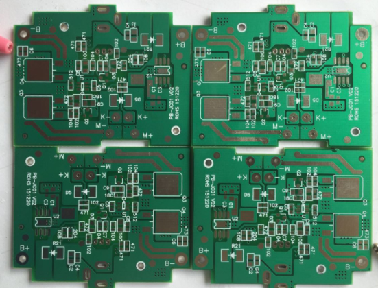
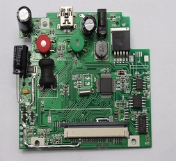
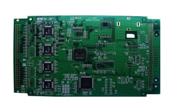
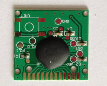
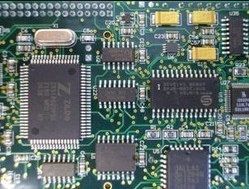
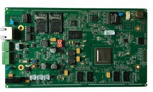
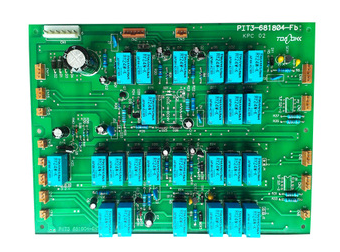
Products that can be processed using SMT include wireless business phone control panels or motherboards, walkie-talkie motherboards, decoder boards, VCD motherboards, MP3 motherboards, car audio motherboards, remote control planes, Doraemon toys, network cards, graphics cards, keyboard boards, and a series of processed products. The price of SMT chip processing is based on the complexity of the processed product, the difficulty of welding, and the number of welding.
How is the desoldering in SMT chip processing done?
How is the desoldering in SMT chip processing done? Come and find out today.
For SMD components with a large number of pins and a wide spacing, a similar method is adopted. First, tin plate on the pad, then use tweezers to hold the component and solder one foot on the left side, and then solder the other foot with tin wire. It is usually better to disassemble these parts with a heat gun. On the one hand, a hand-held hot air gun is used to melt the solder. On the other hand, when the solder is melted, a clamp such as tweezers is used to remove the components.
For components with high pin density, the welding process is similar, that is, one leg is welded first, and then the remaining legs are welded with tin wire. The number of feet is large and dense, and the alignment of the nails and pads is the key. Normally, the pads on the corners are plated with very little tin, and the parts are aligned with the pads with tweezers or hands. The edges of the pins are aligned. These components are pressed slightly harder on the printed circuit board, and the corresponding pins on the pads are soldered with a soldering iron.
Patch processing red glue is a chemical compound, the main component is polymer materials. Patch processing fillers, curing agents, other additives, etc. Patch processing red glue has viscosity fluidity, temperature characteristics, wetting characteristics and so on. According to the characteristics of patch processing red glue, in production, the purpose of using red glue is to make the parts firmly stick to the surface of the PCB to prevent them from falling.
For SMD components with a small number of pins, such as resistors, capacitors, bipolars and triodes, first tin plating on a pad on the PCB, then use tweezers to clamp the component to the mounting position with your left hand and fix it on the PCB On the circuit board, solder the pins on the pads to the sold pads with your right hand. iron. The left-hand tweezers can be loosened, and the remaining feet can be soldered with tin wires. This type of component is also easy to disassemble, as long as both ends of the component and the soldering iron are heated at the same time, and the tin is melted and lifted slightly to disassemble.
SMD processing red glue is a purely consumable material and is not a necessary process product. Now with the continuous improvement of surface mount design and technology, SMT processing through-hole reflow soldering and double-sided reflow soldering have been realized. The placement process of chip processing patch adhesive is showing a trend of less and less.