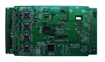
Advantages of SMT chip processing technology
What are the advantages of SMT chip processing technology:
1. High reliability and strong anti-vibration ability
SMT chip processing uses chip components with high reliability. The components are small and light, so it has strong anti-vibration ability. It adopts automated production and has high mounting reliability. Generally, the rate of bad solder joints is less than 10 parts per million. The wave soldering technology of through-hole plug-in components is one order of magnitude lower, which can ensure a low defect rate of solder joints of electronic products or components. At present, almost 90% of electronic products adopt SMT technology.
2. Electronic products are small in size and high in assembly density
The volume of SMT chip components is only about 1/10 of the traditional plug-in components, and the weight is only 10% of the traditional plug-in components. Usually, the use of SMT technology can reduce the volume of electronic products by 40%~60% and the quality by 60%~80 %, the occupied area and weight are greatly reduced.

The SMT patch processing assembly component grid has developed from 1.27MM to the current 0.63MM grid, and individual grids have reached 0.5MM. The through-hole mounting technology is used to install the components, which can make the assembly density higher.
3. Good high frequency characteristics and reliable performance
Because the chip components are firmly mounted, the devices are usually leadless or short leads, which reduces the influence of parasitic inductance and parasitic capacitance, improves the high-frequency characteristics of the circuit, and reduces electromagnetic and radio frequency interference. The high frequency of the circuit designed with SMC and SMD is up to 3GHz, while the chip component is only 500MHz, which can shorten the transmission delay time. It can be used in circuits with a clock frequency above 16MHz. If the MCM technology is used, the high-end clock frequency of the computer workstation can reach 100MHz, and the additional power consumption caused by parasitic reactance can be reduced by 2-3 times.
Analysis report of poor wettability of PCB pads
The following is an analysis report of PCB pads:
1. Sample description
After the electrical performance test of the PCBA samples submitted for inspection, it is found that the BGA part may have poor soldering (suspected virtual soldering). Now it is necessary to analyze whether the problem is caused by the PCBA in the SMT process or the cause of the PCB (that is, poor soldering). One PCBA sample and 3 PCB samples used.
2. Analysis process
1. Microscopic analysis
Cut the BGA part on the PCBA, use epoxy resin to inlay, plan, polish, and etch the metallographic section or cross-section of the BGA solder joint, and then use Nikon OPTIPHOT metallographic microscope and LEICA MZ6 stereo microscope to observe and analyze. The fourth solder joint in the first row has a defect, and there is a clear separation between the solder ball and the pad (Figure 1). Similar conditions have not been checked for other solder joints.
2. Solderability analysis of PCB pads
3. PCB surface condition analysis
4. SEM and EDX analysis
5. Analysis of the wettability of solder paste
3. Conclusion
After the above analysis, this conclusion can be drawn:
The fourth solder joint in the first row of the BGA part of the PCBA sample has a bad defect, and there is an obvious open circuit between the solder ball solder joint and the pad.
The reasons for the open circuit are: poor wettability (solderability) of the PCB pad, and there are unknown organic matter on the surface of the pad. The organic matter is insulated and solder resist, so that the BGA solder ball cannot form a metallization layer with the pad during soldering.