What are the main aspects of SMT chip processing progress?
The progress of SMT processing is mainly reflected in four aspects: First, the product is compatible with the development of new assembly materials; the second is the product assembly is compatible with the new surface assembly components; the third is the high-density assembly, three-dimensional assembly, and micro-electromechanical system. The assembly requirements of new assembly forms such as assembly are adapted; the fourth is that the SMT process modern electronic products have many varieties and are adapted to the characteristics of fast update. The details are as follows:
1. The installation orientation of SMT process is extremely strict, and the surface assembly process technology with special assembly requirements such as product accuracy requirements is also the content that needs to be studied in the future, such as the surface assembly of electromechanical systems, etc.;
2. With the fine pitch of component pins, the micro-assembly technology of 0.3mm pin pitch in SMT processing technology has become mature, and at the same time, it is developing in the direction of improving assembly quality and increasing the pass rate of assembly;
3. The SMT process is the assembly process technology that is suitable for high-density assembly and three-dimensional assembly. It is now planned as the main content that needs to be studied in the next period;

4. In order to adapt to the assembly requirements of multi-variety, small batch production and rapid product update, rapid assembly process reorganization technology, assembly process optimization technology, and assembly design and manufacturing integration technology are constantly being proposed and researched.
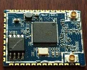
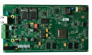
Package type and process flow in SMT chip processing
SMT chip processing has different package types. Different types of SMT chip processing components have the same shape, but the internal structure and use are very different. For example, TO220 packaged components may be triode, thyristor, field effect transistor, Or double diode. TO-3 packaged components include transistors, integrated circuits, etc. There are also several types of packages for diodes, glass package, plastic package and bolt package. Diode types include Zener diodes, Rectifier diodes, Tunnel diodes, Fast recovery diodes, Microwave diodes, Schottky diodes, etc. All of these diodes use one or more types. Package.
Classification of different technological processes in SMT patch factory:
1. Solder paste-reflow soldering process
Solder paste-reflow soldering process flow. The characteristics of the process flow are: simple, fast, and conducive to the reduction of product volume, and the process flow shows superiority in the lead-free process.
2. SMT patch-wave soldering process
SMD-wave soldering process flow. The characteristics of the process flow are: the use of double-panel space, the volume of electronic products can be further reduced, and part of the use of through-hole components, low prices. The equipment requirements increase, and there are many defects in the wave soldering process, making it difficult to achieve high-density assembly.
3. Double-sided solder paste-reflow soldering process
Double-sided solder paste-reflow soldering process. The characteristics of the process flow are: double-sided solder paste reflow soldering process, which can make full use of PCB space, is the only way to minimize the installation area. The process control is complicated and the requirements are strict. It is often used in intensive and ultra-small electronic products. The telephone is one of the typical products. However, this process is rarely recommended in the Sn-Ag-Cu lead-free process, because the high temperature of the two soldering will cause damage to the PCB and components.
4. Mixed installation process
Mixed installation process. The characteristics of this process flow are: making full use of the PCB double-sided space is one of the methods to minimize the installation area. The advantage of keeping the through-hole components is cheap, which is more common in the assembly of consumer electronic products.