14 precautions for board casting and printing before SMT chip processing
We are very strict in the management of the SMT chip processing process, whether it is the rewarming and stirring of the solder paste, the scrubbing of the steel mesh, the first piece verification, the feeding verification, and the IPQC inspection, after arriving the furnace AOI 100 % Of the testing, we are strictly in accordance with the ISO9001:2008 system standards, and continue to improve. Through cooperation and efforts with customers, our direct rate can reach more than 98%.
The PCB must be counted without unpacking before putting it in to prevent shortage of original packaging;
2. For PCBs with BGA parts, 100% inspection of the pads must be made before the input to confirm that there is no foreign matter, dirt, oxidation, etc.;
3. Do not directly touch the PCB when taking the PCB, especially in mobile phone products and OSPs, the PCB must use finger cots;
4. Set relevant printing parameters according to process requirements;
5. Add solder paste several times in small amounts, the diameter of the solder paste rolling on the stencil is best to keep 1.0-1.5cm;

6. Clean the steel mesh as required, manually clean it in one hour, clean the solder paste in the packaging screen frame, and clean it with ultrasonic for six hours;
7. OSP PCB must be produced within 24 hours, too long time will cause serious oxidation of PCB;
8. The thickness of solder paste is tested by IPQC every 2 hours;
9. Before opening the production line, the printing personnel need to use: steel mesh, scraper, solder paste, and special machine types also need jig production;
10. After the production is completed, the printer will clean the stencil and scraper and return it to the tool room together with the unused solder paste;
11. The solder paste must be warmed up for 4 hours before it can be used, and it must be returned to the refrigerator if it is not used for more than 24 hours;
12. The solder paste must be mixed with a special mixer.
13. The storage conditions of solder paste are: 5-10 degrees Celsius, 6 months from the production date;
14. The use period of solder paste added to the stencil is 12 hours, and the unused period is 48 hours after opening the lid.
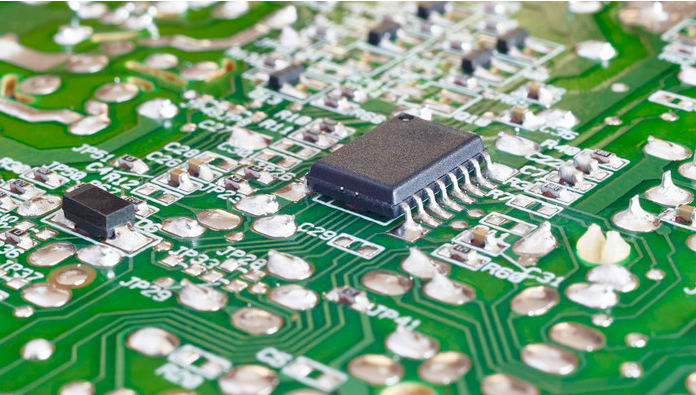
Quickly distinguish common SMT patch components
With the development of SMT patch technology towards miniaturization and high efficiency, various commonly used components are getting smaller and smaller. The commonly used chip resistors, chip inductors and chip capacitors have become difficult to distinguish in appearance. So how to quickly distinguish the commonly used SMT components? Below, the technicians of Jingbang Technology will introduce you the method of quick distinction. 1492679352965056247 [1]
1. The difference between chip inductors and chip capacitors:
(1) Look at the color (black)-generally black is a chip inductor. SMD capacitors are black only for SMD tantalum capacitors in precision equipment, and other ordinary SMD capacitors are basically not black.
(2) Look at the model code-chip inductors start with L, and chip capacitors start with C. Preliminarily judging from the circular shape, it should be an inductance. If the resistance at both ends of the measurement is a few tenths of an ohm, it is an inductance.
(3) Detection-chip inductors generally have small resistance, and there is no back and forth deflection of the multimeter pointer caused by "charge and discharge". The chip capacitor has a charging and discharging phenomenon.
(4) Look at the internal structure-if you find the same components, you can split the components to see the internal structure. The coil structure is the chip inductor.
2. The difference between chip inductors and chip resistors:
(1) Judging from the shape-the shape of the inductor is polygonal, while the resistance is basically rectangular. When the shape of the component to be distinguished has a polygonal shape, especially a circular shape, it is generally regarded as an inductor.
(2) Measure the resistance value-the resistance value of the inductor is relatively small, and the resistance value of the resistor is relatively large.
3. The difference between chip capacitors and chip resistors:
(1) Look at the color-chip capacitors are mostly gray, cyan-gray, and yellow, and are usually slightly lighter than the cardboard shell. Some chip capacitors are not printed, mainly because they are sintered at a high temperature, which makes it impossible to print on their surface.
(2) Look at the logo-the symbol of the chip capacitor in the circuit is "C", and the symbol of the chip resistor is "R".
(3) Measurement method-Generally, the resistance of the chip capacitor is very large, while the chip resistance is relatively small. SMD capacitors have charging and discharging phenomena, while SMD resistors do not.
As long as you are familiar with the functions and models of various SMT components, you can quickly distinguish various components with similar ppearances.