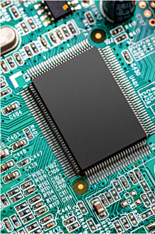
PCBA circuit board processing is an indispensable step in the design and production process of electronic equipment. PCBA circuit board carries the control system of electronic equipment. Its quality directly affects the operation of electronic equipment and product quality. A good product cannot do without High-quality PCBA circuit board support, and in the PCBA circuit board processing, some problems will inevitably be encountered. With the rapid development of SMT technology and component high-sealing technology, the quality and reliability of its solder joints are tested Testing technology must also adapt to the needs of this development. New technologies using various advanced testing and testing equipment are also emerging one after another, but the high price and maintenance difficulties also make most companies in the industry unaffordable.
Basic principles of dyeing and penetration test
Put the solder joints in red ink or dye, and let the red ink or dye penetrate into the cracks of the solder joints. After drying, the solder joints are forcibly separated. The solder joints usually crack from the weak links (cracks), so they can pass the inspection The dyeing area and interface of the interface at the cracking point are used to judge the size and depth of the crack, and the interface of the crack, so as to obtain the quality information of the solder joint.

Dyeing and penetration test method description sample preparation
First, carefully cut the sample to be tested from the circuit board assembly PCBA. "If the PCBA is not large! You can also test the entire PCBA containing the device to be tested! But to do this, you need to have a large enough red ink Containers may also waste more red ink. If the price of red ink becomes more expensive, the cost will increase." However, direct interception of samples also requires special care. Special tools can be used to avoid damage to the tested samples. Destruction or damage of solder joints"
Dyeing and penetration
After the sample is prepared, you can directly place the sample in a container filled with red ink, close it tightly, and then draw a vacuum. Generally, it can be pumped to a pressure of 100 millibar (mbar). Come out and let the red ink penetrate where it should go and dye it red. "Usually in order to make the red ink have a better penetration effect, a few drops of surfactant are often added to the red ink to reduce its surface tension."
bake
The dyed sample waits for the excess red ink to drain! Put it into an oven at a temperature of about 100 degree Celsius, and bake it until the sample is dry. The time depends on the nature of the red ink used. It usually takes one hour, the fastest It takes 15 minutes! The longest time is even more than an hour to dry. "Dryed samples usually need to be placed in a desiccator to cool to room temperature! To avoid moisture absorption"
Device separation
The dyed device can be separated by various tools! To check whether the solder joint has a red-stained interface" The method of separation is generally to use L-shaped steel hooks to first tilt the four corners of the device, and bend the PCBA to make The solder joints of the device are partially broken" and then use super glue to fix a steel cylinder of appropriate size on the surface of the device (see Figure 1). After fixing the PCBA where the device is located, extend the steel cylinder vertically to separate it.
Device% If the device is too large or too strong, you can use the method of occupying the hole and exerting force as shown in Figure 2. Some people suggest to use the method of heating up to 140 degree Celsius; or the method of heat preservation when the device is difficult to separate! But the actual operation is very troublesome or difficult ! It is rarely used in the industry.
Check and record
Use a stereo or metallurgical microscope with sufficient magnification to inspect the interface of the device after separation. "Note that the two surfaces of the separated PCB and the device should be checked symmetrically. Note that the interface dyed in red should be photographed and recorded. Generally, they are symmetrical, that is, PCB. The interface between the surface and the device pin will be dyed red or not at the same time." It is particularly reminded that the red-stained interface (failure or separation mode) and area of the solder joint must be carefully recorded, and the solder joint is in all the solder joints of the entire device. Distribution law of%
Analysis and Application of Dyeing and Penetration Test Results
Through the dyeing test, we can get information about the quality of PCBA solder joints, especially the information on the separation interface and its distribution can obtain the basis for process improvement, and even distinguish the responsibility for quality accidents.