Reflow soldering is the final process of the SMT production process. Its defects combine the defects of printing and patching, including less tin, short circuit, side standing, offset, missing parts, multiple parts, wrong parts, reverse, reverse, and vertical Stele, cracks, tin beads, voids, voids, gloss, among which tombstones, cracks, tin beads, voids, voids, and gloss are unique defects after welding.
Tombstone: The phenomenon that one end of the component leaves the pad and rises diagonally or upright.
Connected tin or short circuit: The solder connection occurs between two or more unconnected solder joints, or the solder of the solder joints and
Adjacent wires are badly connected.
Displacement/offset: The component deviates from a predetermined position in the horizontal (horizontal), vertical (vertical) or rotational direction of the pad.
Empty welding: the assembly phenomenon that the solderable end of the component is not connected to the pad.
Reverse: Wrong direction when mounting polarized components.
Wrong part: The type and specification of the component mounted in the specified position does not meet the requirements.
Few pieces: no material is required to be placed where there are components.
Exposure of copper: The green oil on the PCBA surface is peeled off or damaged, and the guiding copper foil is exposed.
Blistering: The deformation of the PCBA/PCB surface due to regional expansion.
Tin hole: After the furnace, there are blow holes and pin holes on the solder joints of the components.
Tin crack: crack on the tin surface.

Hole plugging: The solder paste remains in the plug-in hole/screw hole, etc. to block the hole.
Warped feet: The feet of multi-pin components are warped and deformed.
Side stand: The side of the component welding end is directly welded.
Weak welding/false welding: The component welding is not strong, and the contact will be poor due to external force or internal stress.
Reverse/reverse white: The component list and the silk screen is pasted on the other side of the PCB, and the product name and specification silk screen font cannot be identified.
Cold welding/non-melting tin: The surface of the solder joints is not shiny, and the crystals are not completely melted to achieve a reliable soldering effect.
Reasons and judgments of displacement, reverse, side stand, missing parts, and wrong parts during the SMT placement process
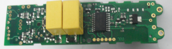
All SMT work is related to welding. On the flow chart of SMT, after the placement machine is welding, this makes the placement machine not only the mechanical equipment with the highest SMT technology content, but also the last quality guarantee before welding. Therefore, the quality of the patch plays a vital role in the entire process of SMT.
In the modern production and processing concept, product quality has become the lifeblood of the company's survival. In the SMT assembly line, after the PCB passes the placement machine, it is about to face the heating and welding forming of reflow soldering, that is to say, the quality of the component's placement directly determines the quality of the entire product. This article will take the real object as a reference, so that relevant SMT practitioners can judge the quality of the patch.
Inferior, and can deal with the defects of the patch in a correct way.
Type of defect Definition Cause of formation Judgment criteria Judgment picture displacement The terminal or electrode piece of the component is removed from the copper foil, which exceeds the judgment standard
1. The mounting coordinates or angles are cheap, and the components are not mounted in the middle of the copper foil.
2. Inappropriate selection of camera recognition method results in poor recognition and transfer.
3. The positioning of the substrate is unstable, the reference point is set improperly or the thimble is improperly caused to shift.
4. The suction position is shifted, causing the suction nozzle to shift when it is not sucked in the middle of the component.
5. The data parameter setting in the parts database is wrong, (such as: the suction nozzle is not set properly), which makes the placement shift
1. The longitudinal or lateral deviation of the component is less than or equal to 1/4 of the width of the component pin, and there are contact pads at both ends of the transverse (longitudinal) direction.
2. There is contact solder paste at both ends of the component.
3. The polarity mark is fuzzy but identifiable,
The direction is correct. The reason for the displacement during the SMT placement process and the judgment standard is reversed. When the component is placed, the polarity of the component does not match the polarity of the corresponding PCB mark.
1. The components are inconsistent before and after the package is built, and the reverse is caused when changing the material.
2. Lead regular components are not installed according to the standard operation during refueling, and the placement machine cannot distinguish, resulting in reverse.
3. Improper setting of the angle of the placement program leads to reverse. All polar components are rejected. The reason for the reverse formation in the SMT placement process and the judgment standard. The side vertical component is being attached to the PCB pad, but the component is rotated 90° or 180° laterally.