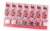
The stencil is also the SMT template (SMT Stencil), which is a special mold for SMT processing. Its main function is to help the deposition of solder paste; the purpose is to transfer an accurate amount of solder paste to the corresponding position of the empty PCB. With the development of SMT technology, SMT steel mesh is also widely used in glue technology such as red glue. Circuit board title=SMT SMT steel mesh production process production process production type "/> The production process of SMT steel mesh can be divided into three types: chemical etching, laser cutting and electroforming.
1. The chemical etching model is etched by a chemical method to form template openings, which is suitable for making brass and stainless steel templates. The specific features are as follows:
1. The opening is bowl-shaped, and the solder paste release performance is not good.
2. It can only be used for the printing of components with a PITCH value greater than 20mil, such as a PITCH value of 25-50mil;
3. The thickness of the template is 0.1~0.5mm;
4. The size error of the hole is 1mil (position error);
5. The price is cheaper than laser cutting and electroforming.
SMT patch stencil etching process
2. The last hole of the laser cutting template uses laser cutting, which has the following characteristics:
1. The openings are naturally trapezoidal up and down, and the upper opening is usually 1~5mil larger than the lower opening, which is conducive to the release of solder paste;

2. The hole size error is 0.3~0.5mil, and the positioning accuracy is less than 0.12mil;
3. The price is more expensive than chemical etching, and cheaper than electroforming;
4. The hole wall is not as smooth as the electroforming template; the thickness of the u5kemanzu template is .12~0.3mm;
6. It is usually used for printing components with a PITCH value of 20mil or less. SMT patch stencil laser engraving process
3. The electroplating molding template uses chemical methods, but instead of etching the required graphics on the metal plate, it directly electroplates the nickel leakage plate, that is, the additive method. Has the following characteristics:
1. Trapezoidal openings are naturally formed, and the hole walls are smooth, which is conducive to the release of solder paste;
2. The protective lip with openings is formed naturally during the production process;
3. It can complete the production of templates with thickness of 2~12mil;
4. Good wear resistance and service life;
5. The price is more expensive and the production cycle is longer.
SMT patch stencil electroformed stencil engraving and engraving process
4. Comparison of the advantages and disadvantages of the three engraving methods. Template types. Etching template. Laser template. Electroforming. Template processing. Chemical etching. Laser cutting. Electroforming. Position precision. ≤15μm≤5μm≤15μm. Shape 2~6 degree Celsius, hole wall roughness, no burr ≤5μm, with fine burr ≤5μm, smooth hole wall, no burr, the service life can be more than 300,000 times and can reach more than 400,000 times
Other features
1. Low production cost and fast production cycle;
2. The accuracy is poor and cannot fully meet the fine-printing requirements
Require
1. The production is more precise;
2. Long production time;
higher cost;
3. Small force between the alloy surface and solder paste makes it easier to peel off