The phenomenon of solder joint peeling mostly occurs in the through-hole wave soldering process, but it has also occurred in the SMT reflow soldering process. The phenomenon is that there is a fault and peeling between the solder joint and the pad. The main reason for this phenomenon is the large difference between the thermal expansion coefficient of the lead-free alloy and the substrate, which causes too much stress in the peeled part when the solder joint is fixed. To separate them, the non-eutectic nature of some solder alloys is also one of the reasons for this phenomenon. Therefore, there are two main ways to deal with this PCB board problem. One is to select an appropriate solder alloy; the other is to control the cooling rate so that the solder joints solidify as soon as possible to form a strong bonding force. In addition to these methods, the magnitude of the stress can also be reduced by design, that is, the copper ring area of the through hole is reduced. A popular method is to use SMD pad design, that is, to limit the area of the copper ring through the green solder mask. However, this approach has two undesirable aspects. One is that the slight peeling is not easy to see; the other is the formation of solder joints between the green oil and the interface of the SMD pad, which is not ideal from the point of view of life. of.
title=The problem of solder joint peeling during SMT chip processing and its solution"/>
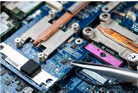
Some peeling phenomenon appears on the solder joints, as shown in the figure below, called cracks or tearing (Tearing). If this problem occurs on the wave through-hole solder joints, some suppliers in the industry consider it acceptable. Mainly because the key parts of the through hole are not in this place. But if it appears on the reflow solder joints, it should be considered a quality problem, unless the degree is very small (similar to wrinkles).
title=The fracture layer on the solder joints in SMT patch processing"/>

The presence of Bi has an impact on both reflow soldering and wave soldering processes, that is, solder joint peeling. Due to the migration characteristics of Bi atoms, only during and after SMT soldering, Bi atoms migrate to the surface and between the lead-free solder and the copper pad, resulting in a "secreted" undesirable thin layer, which is accompanied by the solder and PCB during use. The CTE mismatch between centralized procurement will cause vertical floating and cracking.
The influence of gold in SMT patch on solder joints
In soldering in the electronics industry, gold has become one of the most commonly used surface coating metals due to its excellent stability and reliability. But as an impurity in the solder, gold is very harmful to the ductility of the solder, because the brittle Sn-Au (tin-gold) intermetallic compound (mainly AuSn4) is formed in the solder. Although the low concentration of AuSn4 can improve the mechanical properties of many Korean tin-containing solders, when the content of gold in the solder exceeds 4%, the tensile strength and elongation at failure will decrease rapidly. The 1.5um thick pure gold and alloy layer on the pad can be completely dissolved into the molten solder during wave soldering, and the formed AuSn4 is not enough to damage the mechanical properties of the disk. However, for the surface assembly process, the acceptable thickness of the gold coating is very low, and accurate calculations are required. Glazer et al. reported that for solder joints between plastic quad flat package (PQFP) and copper-nickel-gold (Cu-Ni-Au) metal plating on FR-4 PCBs, when the gold concentration does not exceed 3.0 W/ O, it will not damage the reliability of the solder joints.
title=The influence of gold and metal compounds in SMT patch on solder joints"/>
Too much IMC endangers the mechanical strength of the solder joints due to its brittleness, and also affects the formation of solder joints. For example, for solder joints formed on the 1.63um gold layer of Cu-Ni-Au pads, 7mil (175um) 91% metal content Sn63Pb37 no-clean solder paste is printed on the pads and then reflowed. The Sn-Au metal compound becomes particles and is widely dispersed in the solder joints.
In PCB processing, in addition to selecting an appropriate solder alloy and controlling the thickness of the gold layer, changing the composition of the base metal containing gold can also reduce the formation of intermetallic compounds.