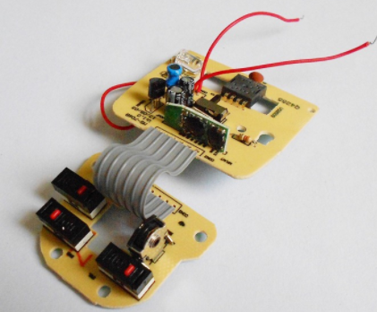
The size of a single PCB should be determined according to the overall structure of the whole machine. The size and shape of the PCB should be suitable for surface assembly production line production, in line with the size range of substrates applicable to printing machines and placement machines, and the working width of reflow soldering furnaces.
Due to the small size of SMB, in order to be more suitable for SMT automated production, multiple boards are often combined into one board, and several PCBs of the same unit are consciously combined into rectangles or squares, which is called puzzle board.
The use of splicing boards for small-sized PCBs can improve production efficiency, increase the applicability of the production line, and reduce tooling preparation costs. Single-sided mounting of the printed circuit board is mounted on the same side, and double-sided full mounting without wave soldering can use the double-numbered front and back sides of the board, and the graphics on both sides are arranged in the same way, this arrangement It can improve equipment utilization (each investment can be halved under the conditions of medium and small batch production), and save production preparation costs and time.
The pieces can be combined by V-groove linear division, stamp hole, punching and other technological means, which require accurate engraving, uniform depth, good mechanical support strength, but easy to be broken by the dividing machine or broken by hand.
The assembly of PCBs with small and identical printed circuits can also be carried out according to this principle, but attention should be paid to the method of compiling component tag numbers.
(1) The stamp board can be composed of multiple same PCBs or multiple different PCBs.
(2) Determine the maximum dimensions of the stamp board according to the situation of the surface assembly equipment, such as the placement area of the placement machine, the maximum printing area of the printing machine and the working width of the reflow conveyor belt.

(3) The connecting ribs between the various circuit boards on the stamp board play the role of mechanical support. Therefore, it must have a certain strength and be easy to break to separate the circuit.
Design of PCB test points and test holes
In order to ensure quality and reduce costs in SMT mass production, online testing is indispensable. In order to ensure the smooth progress of the test work, the design of the test points and test holes (electrical connection holes used for the electrical performance testing of PCB and PCB components) should be considered during PCB design.
(1) Contact reliability test design. In principle, the test points should be located on the same surface and be evenly distributed. The diameter of the pad at the test point is 09mm ~1.0mm, and it is matched with the relevant test pin. The center of the test point should fall on the grid, and be careful not to be designed within 5mm of the edge of the board, and the center distance between adjacent test points should not be less than 1.46mm.
PCB test point and test hole design contact reliability test design
No other components should be designed between the test points, and the distance between the test point and the component pad should not be less than 1mm to prevent short circuits between the components or test points, and note that the test points cannot be coated with any insulating layer.
Design of PCB test points and test holes
In principle, the test holes can be replaced by process holes, but the test holes should still be designed on the daughter board when testing the single board of the jigsaw.
(2) Electrical reliability test design, all electrical nodes should provide test points, that is, test points should be able to cover all I/0, power ground and return signals, and each IC should have power and ground test points. If the device has more than one power supply and ground pin, test points should be added separately. The power supply and ground of an integrated block should be placed within 2.54mm, and the IC control line cannot be directly connected to the power supply, ground or common resistance. VLSI and ASIC devices with boundary scan devices should be added as auxiliary test points to realize boundary scan functions, such as clock, mode, data serial input/output terminal, reset terminal, in order to test the internal functional logic of the device itself. Require.