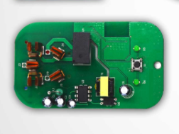
Incoming inspection that needs to be done before SMT patch processing
The inspection before SMT chip processing is the primary condition to ensure the quality of the chip. The quality of components, printed circuit boards, and smt chip materials directly affect the quality of the PCB board. Therefore, the electrical performance parameters of components and the solderability of soldering tips and pins, the productivity design of printed circuit boards and the solderability of pads, solder paste, patch glue, rod-shaped solder, flux, cleaning The quality of smt patch materials such as agents must have strict incoming inspection and management systems. The quality problems of components, printed circuit boards, and smt patch materials are difficult to solve in the subsequent process.
Let's introduce what kind of inspection work is done before processing.
1. Inspection of smt components:
The main inspection items of components include: solderability, pin coplanarity and usability, which should be sampled by the inspection department. To test the solderability of components, stainless steel tweezers can hold the component body and immerse it in a tin pot at 235±5 degree Celsius or 230±5 degree Celsius, and take it out at 2±0.2s or 3±0.5s. Check the soldering end of the solder under a 20 times microscope, and it is required that more than 90% of the soldering end of the component is soldered.

The patch processing workshop can do the following visual inspections:
1. Visually or with a magnifying glass, check whether the solder ends or pin surfaces of the components are oxidized or have no contaminants.
2. The nominal value, specification, model, accuracy, and external dimensions of the components should be consistent with the product process requirements.
3. The pins of SOT and SOIC cannot be deformed. For multi-lead QFP devices with a lead pitch of less than 0.65mm, the pin coplanarity should be less than 0.1mm (optical inspection by the placement machine).
4. For products that require cleaning, the mark of the components will not fall off after cleaning, and will not affect the performance and reliability of the components (visual inspection after cleaning).
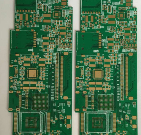
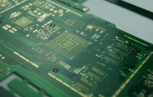
2. Printed circuit board (PCB) inspection
(1) The PCB land pattern and size, solder mask, silk screen, and via hole settings should meet the design requirements of SMT printed circuit boards. (Example: Check whether the pad spacing is reasonable, whether the screen is printed on the pad, whether the via is made on the pad, etc.).
(2) The external dimensions of the PCB should be consistent, and the external dimensions, positioning holes, and reference marks of the PCB should meet the requirements of the production line equipment.
(3) PCB allowable warpage size:
1. Upward/convex surface: maximum 0.2mm/5Omm length and maximum 0.5mm/the length direction of the whole PCB.
2. Downward/concave surface: maximum 0.2mm/5Omm length and maximum 1.5mm/the length direction of the whole PCB.
(4) Check whether the PCB is contaminated or damp
As for the quality of smt patch materials, I believe that most patch processing plants will have no problems. The above is the inspection work before the start of patch processing. I hope friends in the electronics industry will also learn more.
SMT chip processing device cracking solution
1. For MLCC capacitors, their structure is made up of laminated ceramic capacitors. Therefore, their structure is weak, low in strength, and has strong heat resistance and mechanical impact, which is especially obvious in wave soldering.
2. During the SMT placement process, the suction and release height of the Z-axis of the placement machine, especially some placement machines that do not have the Z-axis soft landing function, the absorption height depends on the thickness of the chip component, not through the pressure sensor, so Tolerances in component thickness can cause cracks.
3. After soldering, if there is warping stress on the PCB, it is easy to cause the components to crack.
4. PCB stress during splicing can also damage components.
5. The mechanical stress during the ICT test caused the device to rupture.
6. The stress during assembly can cause damage to the MLCC around the fastening screw.
SMT chip processing device cracking scheme
1. Carefully adjust the welding process curve, especially the heating speed should not be too fast.
2. During the placement, please ensure proper placement of the machine pressure, especially for thick plates and metal substrates, as well as ceramic substrates to mount MLCC and other brittle devices, pay special attention to
3. Pay attention to the placement method and shape of the cutter.
4. The warpage of the PCB, especially the warpage after soldering, should be specially corrected to prevent the stress caused by the large deformation from affecting the device.
5. During PCB design, avoid high stress areas of MLCC and other devices.